Flash memory and manufacturing method thereof

A memory and flash technology, applied in the field of non-volatile semiconductor memory, can solve the problems of leakage current, affect the use range of flash memory, small channel current, etc., achieve low power consumption, suppress source-drain punch-through effect, and solve work problems. low current effect

Inactive Publication Date: 2012-10-17
PEKING UNIV
View PDF4 Cites 6 Cited by
  • Summary
  • Abstract
  • Description
  • Claims
  • Application Information

AI Technical Summary

Problems solved by technology

For this reason, TFET-based flash memory requires special attention when programming, so as not to over-program and inject too many electrons into the floating gate, and the resulting negative potential makes the entire device operate without

Method used


Image

  • Flash memory and manufacturing method thereof
  • Flash memory and manufacturing method thereof
  • Flash memory and manufacturing method thereof

Examples


Embodiment Construction

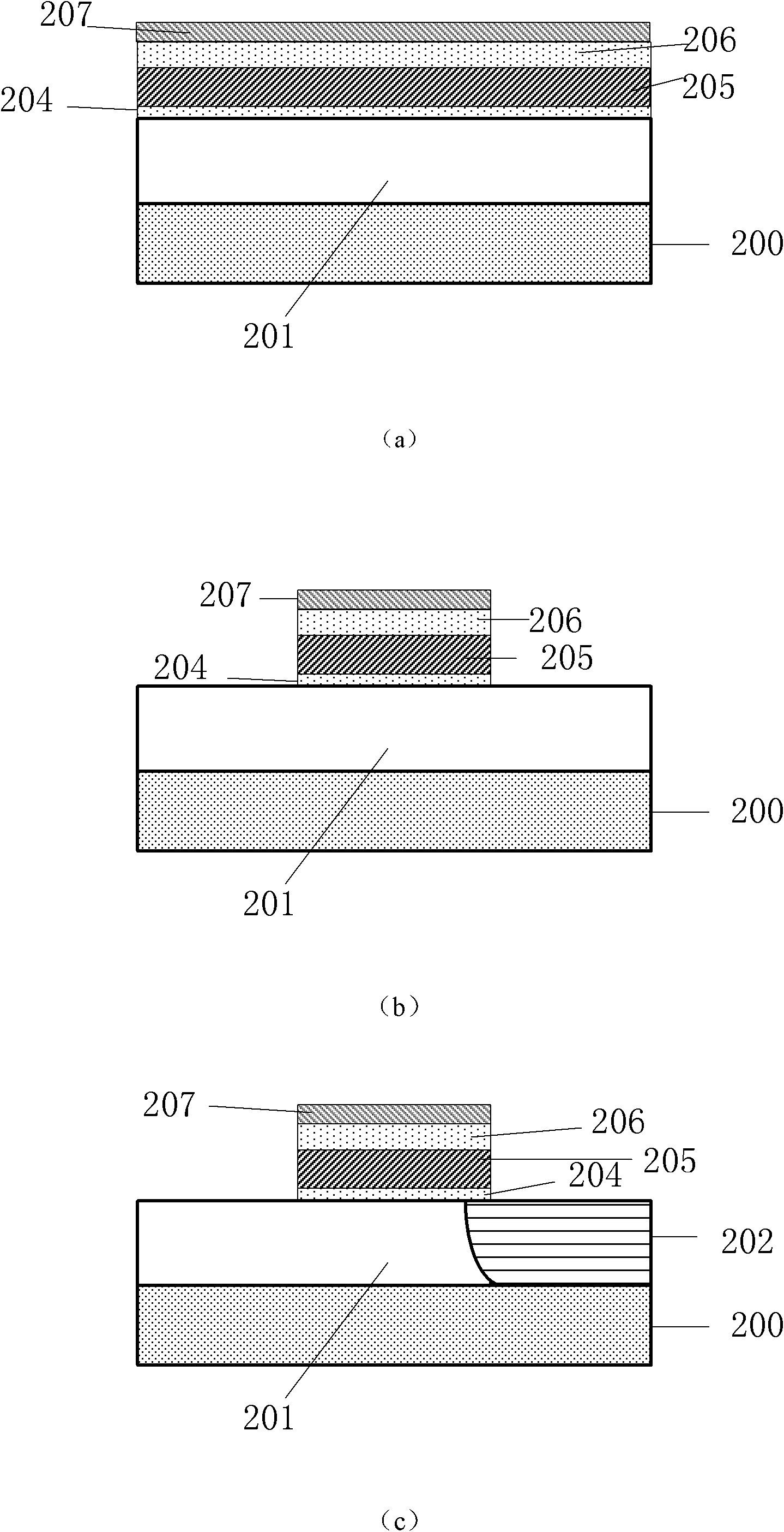
[0037] Below in conjunction with accompanying drawing, further illustrate the preparation of flash memory of the present invention

[0038] The preparation of above-mentioned flash memory comprises the following steps:

[0039] 1) Single throw SOI silicon substrate, shallow trench isolation (STI);

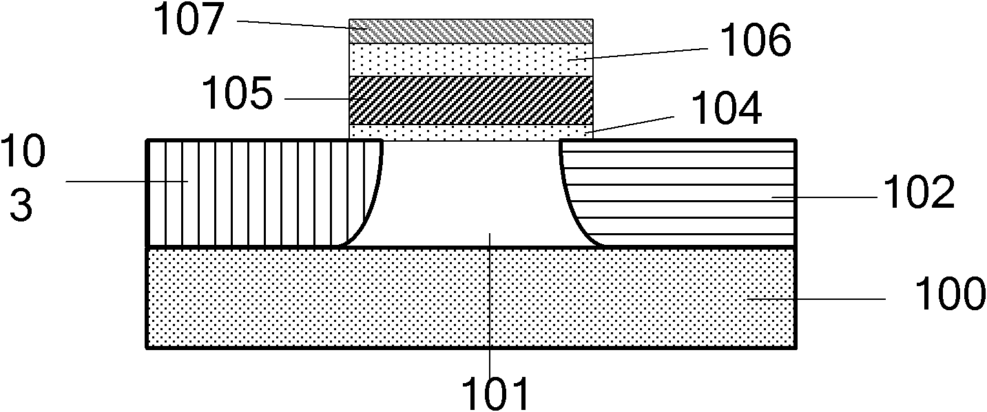
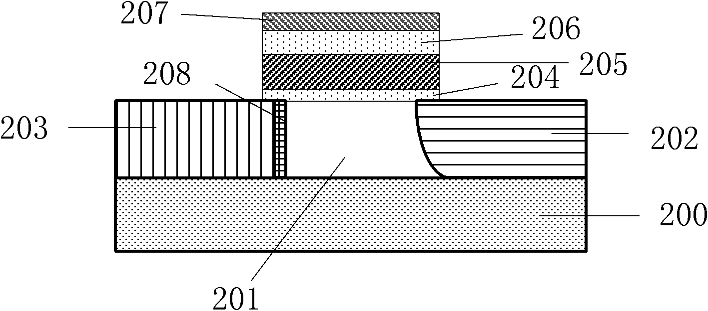
[0040] 2) A sacrificial oxide layer is thermally grown to improve the surface quality of the channel, and the sacrificial oxide layer is rinsed off with hydrofluoric acid. Then thermally grow an oxide layer of 8 nanometers 204 (tunneling oxide layer), and then deposit a polysilicon layer of 90 nanometers, and heavily dope the polysilicon layer to form a floating gate structure 205;

[0041] 3) Deposit oxide layer 10 nanometers 206 (barrier oxide layer) and polysilicon 50 nanometers polysilicon afterwards, form as image 3 (a) structure;

[0042] 4) heavily doping the top polysilicon, followed by rapid thermal annealing (RTA) to activate the impurities in the control gate 207 and...


PUM


Abstract

The invention discloses a flash memory and a manufacturing method thereof, belonging to the technology field of a semiconductor memory. The flash memory includes a buried oxide layer on which a source terminal, a channel and a drain terminal are arranged. The channel locates between the source terminal and the drain terminal. A tunnel oxide layer, a polysilicon floating gate, a barrier oxide layer and a polysilicon controlling gate are arranged on the channel in order. A thin silicon nitride layer is arranged between the source terminal and the channel. The manufacturing method comprises the following steps of: (1) providing an SOI silicon substrate with shallow trench isolation and forming an active area; (2) growing the tunnel oxide layer and a first polysilicon layer on the silicon substrate in order and preparing the polysilicon floating gate, and growing the barrier oxide layer and a second polysilicon layer and preparing the polysilicon controlling gate; (3) etching and forming a gate stacking structure; (4) preparing the drain terminal on one side of the gate stacking structure, etching a thin silicon film on the other side of the gate stacking structure, growing the thin silicon nitride layer, then backfilling a material of silicon, and preparing the source terminal. The flash memory and the method have the advantages of high programming efficiency, low power consumption, and capability of inhibiting a source-drain punch-through effect effectively.

Description

technical field [0001] The invention belongs to the technical field of non-volatile semiconductor memory in VLSI, and in particular relates to an improved TFET (Tunneling Field Effective Transistor)-based flash memory and a preparation method thereof. Background technique [0002] With the rapid development of the semiconductor industry, a large number of various consumer electronic products have emerged. As an important part of the storage part, non-volatile semiconductor memory is also widely used in various electronic products, and its performance requirements are becoming more and more stringent. [0003] Flash memory (Flash Memory, also called flash memory) is a non-volatile semiconductor memory widely used in the industry. In order to meet the needs of each generation of technology, this kind of memory has been making some improvements including structure, material, working mechanism and so on. However, with the continuous shrinking of process nodes and the emergence...

Claims


Application Information

Patent Timeline
IPC IPC(8): H01L27/115H01L21/8247G11C16/04
CPCH01L29/7391H01L29/66825H01L29/788H01L29/8616
Inventor 秦石强黄如蔡一茂唐粕人谭胜虎
Owner PEKING UNIV
Why Eureka
Try Eureka