Green light emitting diode and manufacturing method thereof

A technology of light-emitting diodes and green light, which is applied to electrical components, circuits, semiconductor devices, etc., can solve the problems of reducing the luminous efficiency of green light-emitting diodes, reducing the luminous efficiency of green light-emitting diodes, and deteriorating electrical properties.

Inactive Publication Date: 2012-10-17
江苏汉莱科技有限公司
View PDF5 Cites 22 Cited by
  • Summary
  • Abstract
  • Description
  • Claims
  • Application Information

AI Technical Summary

Problems solved by technology

The In(Al)GaN material with high In composition is easy to cause the phase separation of In, which makes the crystal quality of In(Al)GaN/(Al)GaN deteriorate. The more the number of quantum wells, the easier it is to generate a large number of defects, thus The luminous efficiency of the green light-emitting diode is reduced, and the electrical properties are deteriorated; at t...

Method used


Image

  • Green light emitting diode and manufacturing method thereof
  • Green light emitting diode and manufacturing method thereof

Examples


Embodiment 1

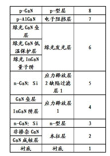
[0023] Such as figure 1 As shown, a high-brightness green light-emitting diode is grown in a MOVCD reaction chamber, and the sapphire substrate 1 is heated to above 1000°C, and the 2 As a carrier gas, treat for 880 seconds, then lower the substrate temperature to 500-600°C, put N 2 Switch to H 2 As a carrier gas, feed TMGa and NH3 to grow a GaN nucleation layer with a thickness of about 35nm; raise the substrate temperature to above 1000°C, use H2 as a carrier gas, and epitaxially grow an unintentionally doped GaN layer of about 1.5 microns; Raise the substrate temperature to above 1060°C, and still use H2 as the carrier gas to grow a 3 micron thick n-type Si-doped GaN layer with a doping concentration of -2.5E+17; reduce the substrate temperature to about 780°C , N2 as the carrier gas, using TEGa as the Ga source, grow an InGaN / GaN quantum well structure with a thickness of about 2000 angstroms on the n-type Si-doped GaN layer to control the stress, and finally control the ...


PUM


Abstract

The invention discloses a green light emitting diode and a manufacturing method thereof. The green light emitting diode is characterized in that a low-temperature protective layer is introduced during epitaxial growth of an InGaN (Indium Gallium Nitride)/GaN (Gallium Nitride) quantum well; the quantum well structure changes from InGaN/GaN to an InGan/Gan low-temperature protective layer 1/GaN structure; thereby protecting In in the InGaN/GaN, and avoiding damage to the In in high-temperature growth, and thus effectively avoiding phase separation of an In component in the InGaN, and improving the internal quantum efficiency; and in addition, two different stress relieving layers are located between an n-type layer and a green light emitting layer, and thus the stress of the green light emitting diode is decreased.

Description

technical field [0001] The invention relates to a green light-emitting diode and a preparation method thereof, and belongs to the field of light-emitting diodes and the preparation method thereof. Background technique [0002] Light-emitting diodes have the advantages of small size, high efficiency and long life, and are widely used in traffic display, indoor and outdoor full-color display and other fields. GaN-based III-V nitrides with wide bandgap and direct bandgap semiconductor materials are due to Its bandgap at room temperature ranges from 0.7eV to 6.2eV, and the corresponding wavelength covers the entire visible light region, infrared region, and ultraviolet region. GaN-based III-V nitride materials have extensive applications in optoelectronic fields such as semiconductor solid-state lighting and full-color display. The application prospect has become a research hotspot in the field of optoelectronics. [0003] The main products of GaN-based light-emitting diodes ar...

Claims


Application Information

Patent Timeline
IPC IPC(8): H01L33/12H01L33/06H01L33/00
Inventor 颜建锋林桂荣庄文荣
Owner 江苏汉莱科技有限公司
Why Eureka
Try Eureka