Thick glue photoetching electroforming technology-based manufacture method of three-dimensional MEMS (micro-electromechanical systems) supercapacitor

A technology for supercapacitors and manufacturing methods, applied in the direction of electrolytic capacitors, capacitors, circuits, etc., can solve the problems of increased integration of liquid electrolytes, low performance of supercapacitors, limited research on supercapacitors, etc., to achieve increased effective surface area, high energy Density, the effect of increasing specific energy and specific power

Active Publication Date: 2012-10-24
GMCC ELECTRONICS TECH WUXI CO LTD
View PDF2 Cites 16 Cited by
  • Summary
  • Abstract
  • Description
  • Claims
  • Application Information

AI Technical Summary

Problems solved by technology

However, there is very limited research on chip-integrated supercapacitors for silicon wafer-level technology or supercapacitors integrated on printed circuit boards.
South Korea's Sung has prepared an all-solid-state supercapacitor with a planar comb structure based on a silicon substrate. However, due to the simple structure and no effective space utilization, the performance of the supercapacitor is not high.
Y.Q. Jiang prepared 80 μm high carbon nanotube forests on silicon wafers as electrodes for supercapa

Method used


Image

  • Thick glue photoetching electroforming technology-based manufacture method of three-dimensional MEMS (micro-electromechanical systems) supercapacitor
  • Thick glue photoetching electroforming technology-based manufacture method of three-dimensional MEMS (micro-electromechanical systems) supercapacitor

Examples


Embodiment Construction

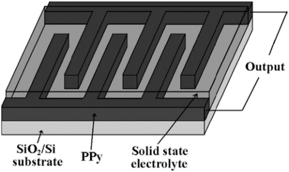
[0029] The structural representation of supercapacitor example of the present invention is as figure 1 shown.

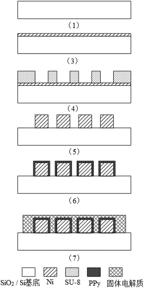
[0030] Such as figure 2 Shown, based on thick glue photolithography electroforming process three-dimensional MEMS supercapacitor manufacturing method, comprises the following steps:

[0031] (1) Select a 4-inch silicon wafer as the substrate, and wash the silicon wafer in xylene, acetone, alcohol, sulfuric acid / hydrogen peroxide, ammonia / hydrogen peroxide, hydrochloric acid / hydrogen peroxide solution to remove oil, oxide film and metal ions.

[0032] (2) Put the silicon wafer cleaned in step (1) into an oxidation furnace for wet thermal oxidation for 10 hours, and the thickness of the oxide layer is 1.5 microns.

[0033] (3) On the silicon wafer oxidized in step (2), a layer of nickel with a thickness of 300 nanometers is sputtered by radio frequency magnetron as an electroforming seed layer.

[0034] (4) Apply a layer of Microchem's SU-8 photoresist on the nicke...


PUM

PropertyMeasurementUnit
Thicknessaaaaaaaaaa
Widthaaaaaaaaaa
Thicknessaaaaaaaaaa

Abstract

The invention relates to a thick glue photoetching electroforming technology-based manufacture method of a three-dimensional MEMS (micro-electromechanical systems) supercapacitor. The supercapacitor has the structure of a comb tooth-shaped inserting finger. The method comprises the following steps of: on the substrate of a silicon wafer, taking SU-8 thick glue photoetching as a temperate, depositing a current collector in the template in an electroforming technology, electrically and chemically polymerizing a conducting polymer on the current collector to be taken as an active electrode material of the supercapacitor, and finally covering a layer of solid electrolyte. The supercapacitor has the three-dimensional structure, so that the superficial area of the electrode can be effectively enlarged, therefore, the energy density and the power density can be greatly improved relative to a flat plate structure. Furthermore, the safety performance of the method can be improved due to the use of solid electrolyte.

Description

technical field [0001] The invention relates to a method for manufacturing a MEMS supercapacitor based on a thick glue photolithography electroforming process. Background technique [0002] Supercapacitor (ultracapacitor) is a new type of energy storage device between traditional capacitors and batteries. It has the advantages of high power density, short charge and discharge time, long cycle life, and good low temperature performance. Ultracapacitors are used in a wide range of military and civilian applications, ranging from micron-level wireless sensors to starting devices for rockets and satellites. According to the latest research by Lux, ultracapacitors have huge market potential, and the revenue of the entire ultracapacitor market is expected to break through from US$208 million in 2008 to US$877 million in 2014. [0003] Small ultracapacitors can be integrated with IC circuits due to portable electronic devices, etc. The supercapacitor integrated with IC current ca...

Claims


Application Information

Patent Timeline
IPC IPC(8): H01G9/155H01G9/038H01G9/058
CPCY02E60/13
Inventor 孙伟陈旭远王俊华
Owner GMCC ELECTRONICS TECH WUXI CO LTD
Why Eureka
Try Eureka