Depletion type power semiconductor device and manufacturing method thereof

A technology of power semiconductors and manufacturing methods, applied in semiconductor/solid-state device manufacturing, semiconductor devices, electrical components, etc., can solve problems such as complex process, large threshold voltage drift, and poor threshold voltage controllability, and achieve simple process, Effect of effective threshold voltage and improvement of flexibility

Active Publication Date: 2012-10-24
HANGZHOU SILAN MICROELECTRONICS
View PDF8 Cites 12 Cited by
  • Summary
  • Abstract
  • Description
  • Claims
  • Application Information

AI Technical Summary

Problems solved by technology

However, this method mainly achieves the purpose of threshold voltage adjustment through selective doping of polysilicon, so the threshold voltage design has little flexibility.
[0005] The U.S. Patent No. 4,786,611 achieves threshold voltage adjustment by diffusion doping polysilicon gate with refractory metal silicide, but the process of this method is relatively complicated, and the controllability of threshold voltage is poor.
[0006] The U.S. Patent No. 3,667,115 grows an oxide layer in the channel region, and uses the "boron" and "phosphorus" characteristics of the oxide layer to invert the channel to manufacture a depletion-mode MOSFET transistor, but the degree of inversion is limited and Difficult to control, poor controllability of threshold voltage, little design flexibility
[0007] The U.S. Patent No. 5,907,777 manufactures a depletion-mode MOSFET by doping the gate dielectric with movable ions, but the reliability of the device is low and the threshold voltage drifts greatly
[0008] Another method in the prior art is to develop a depletion transistor by performing reverse ion implantation on the channel region. Since it only performs selective reverse ion implantation on the channel region, an additional mask is required to increase the cost

Method used


Image

  • Depletion type power semiconductor device and manufacturing method thereof
  • Depletion type power semiconductor device and manufacturing method thereof
  • Depletion type power semiconductor device and manufacturing method thereof

Examples


Embodiment Construction

[0062] The present invention will be further described below in conjunction with specific embodiments and accompanying drawings, but the protection scope of the present invention should not be limited thereby.

[0063] figure 1 A schematic flow chart showing a method for manufacturing a depletion-mode power semiconductor device in this embodiment includes the following steps:

[0064] Step S11, providing a semiconductor substrate;

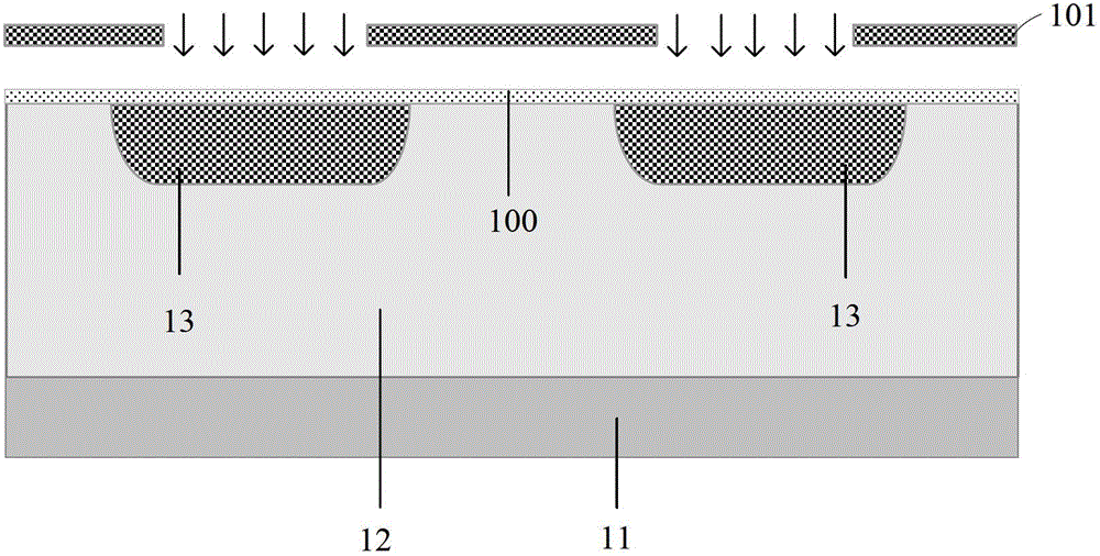
[0065] Step S12, forming an epitaxial layer of the first doping type on the semiconductor substrate;

[0066] Step S13, using a well region implantation mask to perform ion implantation on the epitaxial layer, the implanted ion type is a second doping type opposite to the first doping type, so as to form a second doping type in the epitaxial layer. Doped type well region;

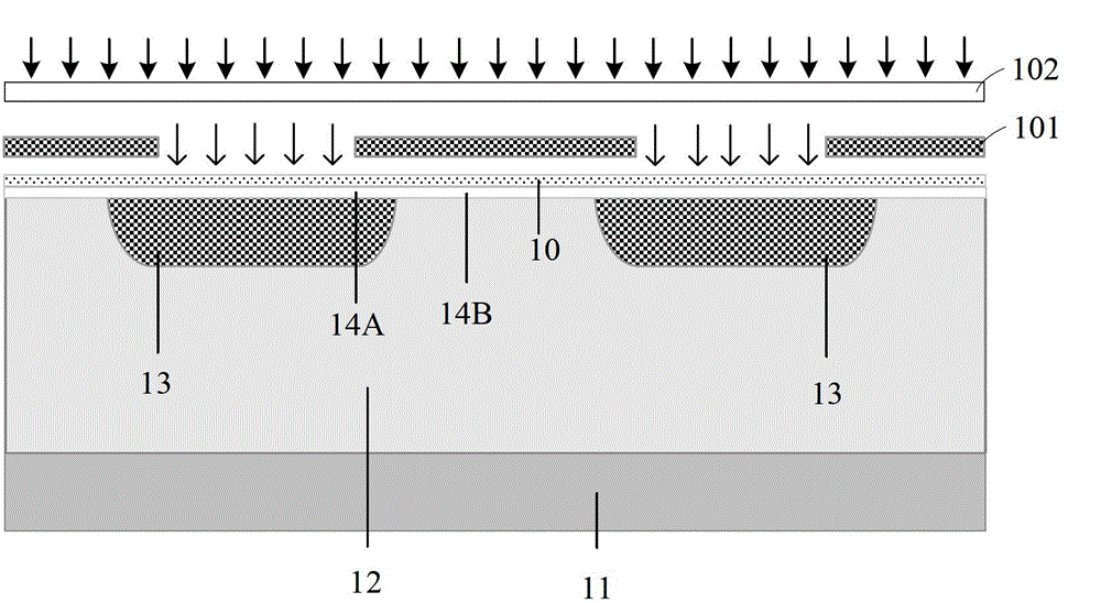
[0067] Step S14, performing ion implantation on the epitaxial layer, the implanted ion type is the first doping type, so as to form an inversion layer with the first doping t...


PUM


Abstract

The invention provides a depletion type power semiconductor device and a manufacturing method thereof. The device comprises a semiconductor substrate, an epitaxial layer of a first doping type, a well region of a second doping type, an inversion layer of the first doping type, a gate dielectric layer and a gate electrode. The well region of the second doping type is formed on the epitaxial layer which is positioned on the semiconductor substrate, the second doping type is opposite to the first dope type, the inversion layer of the first doping type is arranged on the surface of the well region, and the gate dielectric layer and the gate electrode are sequentially positioned on the epitaxial layer. The distance of the well region extending below the gate electrode is 0.75XXj+b, wherein Xj refers to the junction depth of the well region, and b is larger than or equal to -2 micrometers and smaller than or equal to 5 micrometers. The depletion type power semiconductor device and the manufacturing method thereof are simple in process procedure, low in cost and high in threshold voltage controllability.

Description

technical field [0001] The invention relates to a depletion type power semiconductor device and a manufacturing method thereof. Background technique [0002] Power semiconductor devices such as MOSFET transistors and IGBT transistors are widely used in medium and high power fields due to their advantages such as high withstand voltage, high current, and low on-resistance. The depletion power semiconductor device (such as MOSFET, IGBT, etc.) is a normally-on device. When in use, its gate G and source S (or emitter E) are connected to a zero-potential device for conduction. After conduction, the source S (or The potential of the emitter E) terminal rises (VS(E)>0), so that the voltage VGS(E)<0 between the gate and the source (or emitter). When VGS(E) (S for MOSFET, E for IGBT) < V TH , the device is automatically turned off, thus simplifying the gate drive and effectively reducing system power consumption. It is widely used in solid state relays, linear amplifiers, ...

Claims


Application Information

Patent Timeline
Patent Type & Authority Applications(China)
IPC IPC(8): H01L29/78H01L29/06H01L21/336H01L21/265
Inventor 叶俊张邵华李敏
Owner HANGZHOU SILAN MICROELECTRONICS
Why Eureka
Try Eureka