LED (Light Emitting Diode) chip provided with stepped current blocking structure and fabricating method thereof

A technology of LED chips and current blocking, applied in circuits, electrical components, semiconductor devices, etc., can solve the problems of reduced electro-optical conversion efficiency of LED chips and poor step coverage of transparent conductive layers, so as to increase electro-optical conversion efficiency and improve current. Diffusion ability, the effect of improving brightness

Active Publication Date: 2012-10-24
宁波安芯美半导体有限公司
View PDF3 Cites 25 Cited by
  • Summary
  • Abstract
  • Description
  • Claims
  • Application Information

AI Technical Summary

Problems solved by technology

[0006] In view of the above-mentioned shortcomings of the prior art, the purpose of the present invention is to provide an LED chip with a stepped current blocking structure and its manufacturing method, which is used to solve the LED chip caused by the poor step coverage of the transparent conductive layer in the prior art. The problem of the reduction of the electro-optical conversion efficiency of the chip

Method used


Image

  • LED (Light Emitting Diode) chip provided with stepped current blocking structure and fabricating method thereof
  • LED (Light Emitting Diode) chip provided with stepped current blocking structure and fabricating method thereof
  • LED (Light Emitting Diode) chip provided with stepped current blocking structure and fabricating method thereof

Examples


Embodiment 1

[0036] like Figure 1 to Figure 4 As shown, the present invention provides a method for manufacturing an LED chip with a stepped current blocking structure, the method at least comprising:

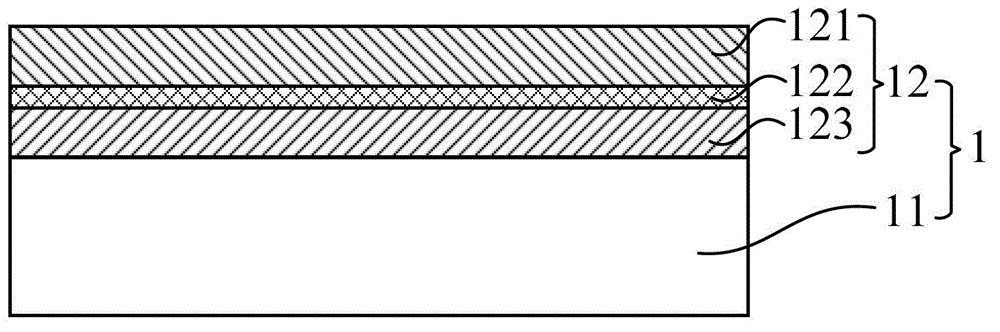
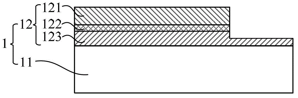
[0037] like figure 1 As shown, step 1) is first performed to provide an LED epitaxial wafer 1. The LED epitaxial wafer 1 at least includes a substrate 11 and a light-emitting epitaxial structure 12 located on the surface of the substrate, wherein the light-emitting epitaxial structure 12 consists of The first conductive type epitaxial layer 121 , the active layer 122 , and the second conductive type epitaxial layer 123 are sequentially included from bottom to bottom.

[0038] It should be pointed out that the material of the substrate 11 includes at least Al 2 o 3(sapphire), GaAs, Si, SiC, GaN, GaP, InP, ZnO, and Ge; formed on the substrate 11 by metal-organic chemical vapor deposition, molecular beam epitaxy, or hydride vapor phase epitaxy The light-emitting epitaxial structure 12; t...

Embodiment 2

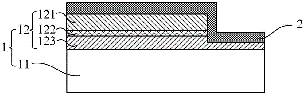
[0057] like Figure 7 As shown, the present invention also provides an LED chip with a stepped current blocking structure, the LED chip at least includes: an LED epitaxial wafer 1, a stepped current blocking structure 2, a transparent conductive layer 3, a first electrode 41, a second Electrode 42, protective layer 5.

[0058] The LED epitaxial wafer 1 at least includes a substrate 11 and a light-emitting epitaxial structure 12 located on the surface of the substrate 11, wherein the light-emitting epitaxial structure 12 includes a first conductivity type epitaxial layer 121, an active layer in sequence from top to bottom. 122, and the second conductivity type epitaxial layer 123.

[0059] Wherein, the material of the substrate 11 includes at least Al 2 o 3 (sapphire), GaAs, Si, SiC, GaN, GaP, InP, ZnO and Ge; the active layer 122 is a single quantum well structure or multiple quantum well structure, quantum dot structure or quantum wire structure ; The epitaxial layer 121 ...


PUM


Abstract

The invention provides an LED (Light Emitting Diode) chip provided with a stepped current blocking structure and a fabricating method thereof. The fabricating method comprises the steps of: providing at least one LED epitaxial wafer comprising a substrate and a light emitting epitaxial structure on the LED epitaxial wafer; fabricating the stepped current blocking structure on the surface of the LED epitaxial wafer vertical to a region of a first electrode correspondingly prefabricated; and fabricating transparent conductive layers on the surfaces of the LED epitaxial wafer and the stepped current blocking structure, and then fabricating a first electrode, a second electrode and a protective layer correspondingly. According to the LED chip provided with a stepped current blocking structure and the fabricating method of the LED chip provided with the stepped current blocking structure provided by the invention, the gradient at the edge of the stepped current blocking structure is slowed so that the contact area of the transparent conductive layer and the stepped current blocking structure is increased, the situation that the transparent conductive layer (ITO) on the side wall (at the step) at the edge of the current blocking structure becomes thinner and even breaks can be avoided, the step covering capacity of the transparent conductive layer is improved, the current spreading capacity of the transparent conductive layer is further improved, the electro-optical conversion efficiency of the LED chip is increased, and the brightness of the LED chip is enhanced.

Description

technical field [0001] The invention relates to an LED chip and a manufacturing method thereof, in particular to an LED chip with a stepped current blocking structure and a manufacturing method thereof. Background technique [0002] LED (Light Emitting Diode) chip, also known as LED light-emitting chip, is the core component of LED lights and a solid-state semiconductor device that can directly convert electrical energy into light energy. The LED chip is mainly composed of two parts, one is a P-type semiconductor, and holes are the majority carriers, and the other is an N-type semiconductor, and electrons are the majority carriers. When the two semiconductors are connected, a P-N junction is formed. When the current acts on the chip through the wire, the electrons will be pushed to the P region, and in the P-N junction region (such as the quantum well region), the electrons will recombine with the holes, and then energy will be emitted in the form of photons. This is the LED...

Claims


Application Information

Patent Timeline
Patent Type & Authority Applications(China)
IPC IPC(8): H01L33/14H01L33/00
Inventor 卢昶鸣
Owner 宁波安芯美半导体有限公司
Why Eureka
Try Eureka