Optical transition layer material, optical substrate/packaging layer, OLED (Organic Light Emitting Diode) and manufacturing methods thereof

A technology of transition layer and encapsulation layer, which is applied in the fields of optical substrate (encapsulation layer), OLED and their respective manufacturing methods, and optical transition layer materials, and can solve problems such as shortening the service life of devices, increasing material costs, and increasing the temperature of organic functional layers. Achieve the effect of improving light extraction efficiency, improving light extraction efficiency, and reducing total reflection loss

Active Publication Date: 2012-10-24
TRULY SEMICON
View PDF2 Cites 24 Cited by
  • Summary
  • Abstract
  • Description
  • Claims
  • Application Information

AI Technical Summary

Problems solved by technology

This situation will bring the following problems: (1) The low light extraction efficiency forces people to use high-grade luminescent materials or increase the input current to meet the requirements of high brightness, which increases the cost of materials and shortens the use of devices life; (2) The energy that cannot be taken out (nearly 80%) will be converted into heat, which will greatly increase the temperature of the organic functional layer, which will not only deteriorate the stability and photoelectric parameter performance of the OLED, but also shorten the life of the OLED; (3) In order to To eliminate the impact of generated heat on OLED performance and lifespan, heat dissipation design must be carried out, which increases production costs
Surface roughening will seriously reduce the light transmittance of glass, so that the effect

Method used


Image

  • Optical transition layer material, optical substrate/packaging layer, OLED (Organic Light Emitting Diode) and manufacturing methods thereof
  • Optical transition layer material, optical substrate/packaging layer, OLED (Organic Light Emitting Diode) and manufacturing methods thereof
  • Optical transition layer material, optical substrate/packaging layer, OLED (Organic Light Emitting Diode) and manufacturing methods thereof

Examples


Embodiment Construction

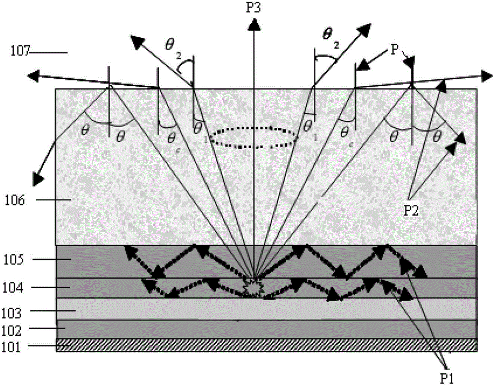
[0051] The basic concept of the present invention is: in order to improve the light extraction efficiency of OLED, prepare a special optical transition layer material, by preparing an optical transition layer on the surface of the substrate (encapsulation layer) of glass and other materials, the optical transition layer is composed of organic material main body layer and Composed of inorganic nanoparticles, it can reduce the total reflection loss of light and greatly improve the light extraction efficiency.

[0052] Key of the present invention is:

[0053] (1) The selection of nanoparticles requires high visible light transmittance, low light absorbance, stable physical and chemical properties (light, heat, water vapor, oxygen), and no reaction with organic carriers, generally wide bandgap semiconductors and insulating oxides , such as SiO 2 , MgO, MgF 2 、TiO 2 , ZnO, Al 2 o 3 , ZrO 2 Wait;

[0054] (2) The selection of organic materials requires high visible light tra...


PUM

PropertyMeasurementUnit
Thicknessaaaaaaaaaa

Abstract

The invention relates to an organic electroluminescent technology and discloses a method for improving the luminous efficiency. The method can be applied to various types of OLED (Organic Light Emitting Diode) devices of bottom emission, top emission, transparency and the like. The invention provides an optical transition layer material, an optical substrate (packaging layer), an OLED, and manufacturing methods thereof. If the OLED is the bottom-emission OLED, an optical transition layer is manufactured on the substrate; if the OLED is the top-emission OLED, the optical transition layer is manufactured on the packaging layer; and if the OLED is the transparent OLED, the optical transition layer can be independently or simultaneously manufactured on the substrate or the packaging layer. An organic material main body with high light transmittance and moderate refractive index and an inorganic nano grain with the high light transmittance and low absorption rate are selected; the inorganic nano grain is used as a scattering medium to be scattered into the organic material main body to prepare the optical transition layer material; and the optical transition layer material is used for preparing an optical transition layer on the substrate (packaging layer) including glass and the like, so that the full-reflection loss of emergent light is effectively reduced and the luminous efficiency of the OLED is improved by 20-50%.

Description

technical field [0001] The invention relates to organic electroluminescence technology, in particular to an optical transition layer material capable of improving light extraction efficiency, an optical substrate (encapsulation layer), OLED and their respective manufacturing methods. Background technique [0002] Organic electroluminescence (OLED, Organic Light-Emitting Diode) is a phenomenon in which organic materials are excited by electrical energy to emit light. An OLED is a "sandwich" structure consisting of an anode, a cathode and a layer of organic material between them. The organic material layer generally includes a hole injection layer, a hole transport layer, a light emitting layer, an electron transport layer, and an electron injection layer. By applying an appropriate voltage between the electrodes, OLED devices can emit light. [0003] see figure 1 , represents the OLED structure and its light propagation path, wherein: the inner surface of the glass substra...

Claims


Application Information

Patent Timeline
IPC IPC(8): H01L51/52H01L51/54H01L51/56
Inventor 何剑张色冯苏君海柯贤军
Owner TRULY SEMICON
Why Eureka
Try Eureka