

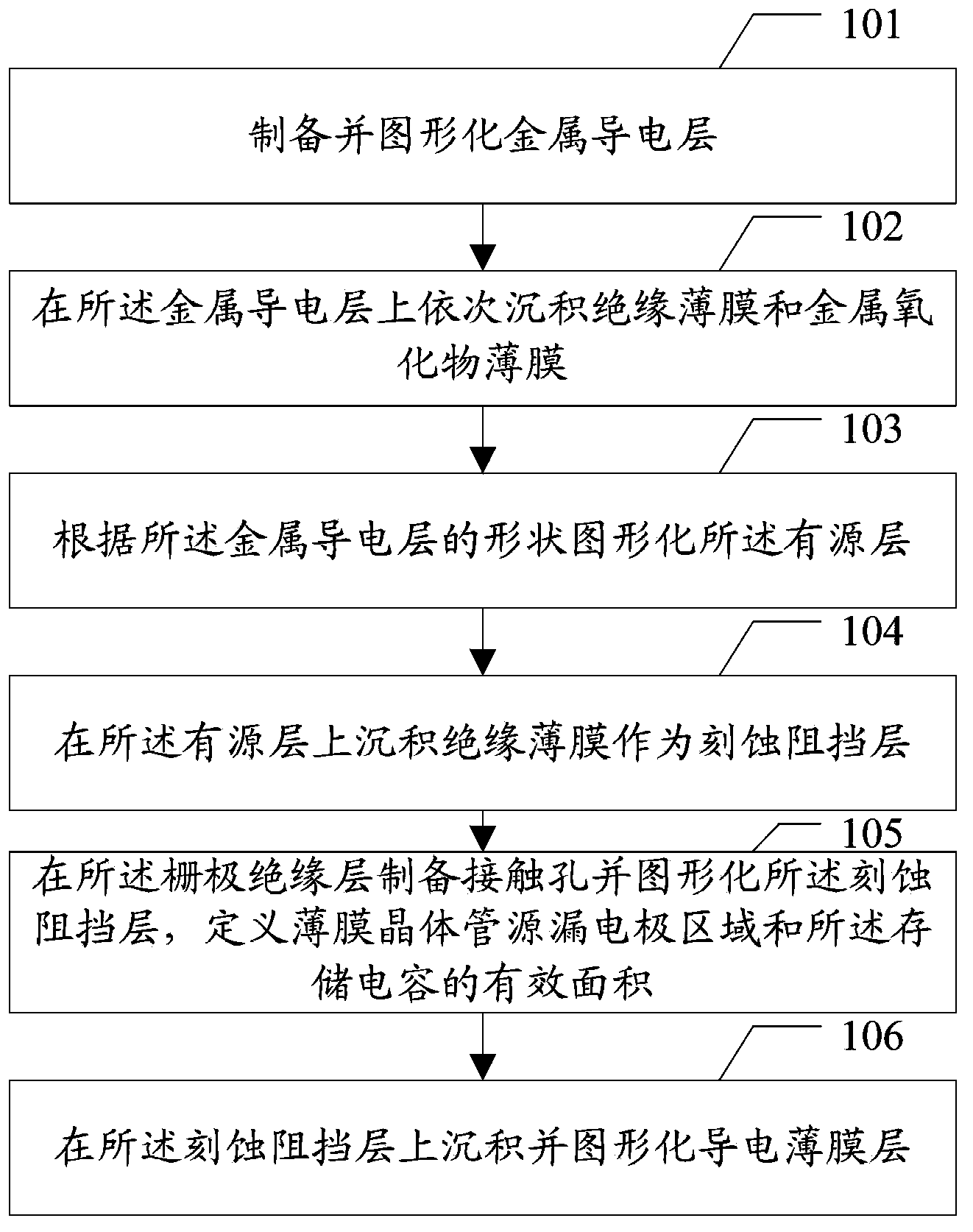
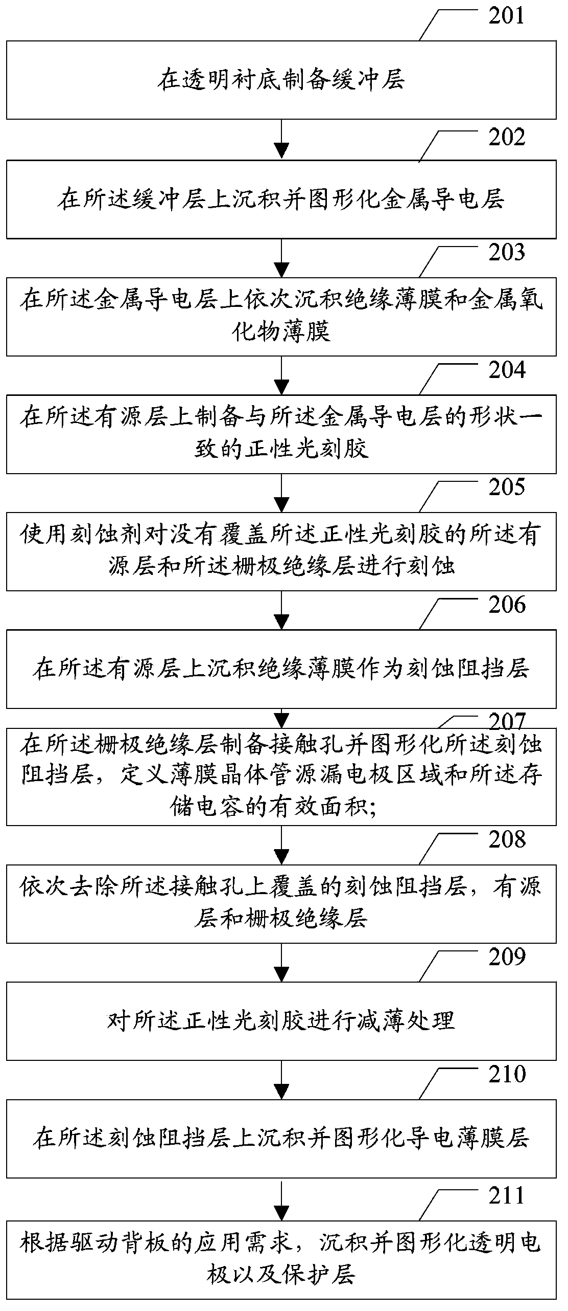
A method of manufacturing a thin film transistor driving backplane
A thin-film transistor and drive backplane technology, which is applied in semiconductor/solid-state device manufacturing, electrical components, circuits, etc., can solve the problems of high production cost, complicated manufacturing process, unfavorable promotion and use, etc., achieve stable performance and reduce interface pollution problems , Reduce the production cost and the effect of process difficulty
- Summary
- Abstract
- Description
- Claims
- Application Information
AI Technical Summary
Problems solved by technology
Method used
Image

Examples
specific example 2
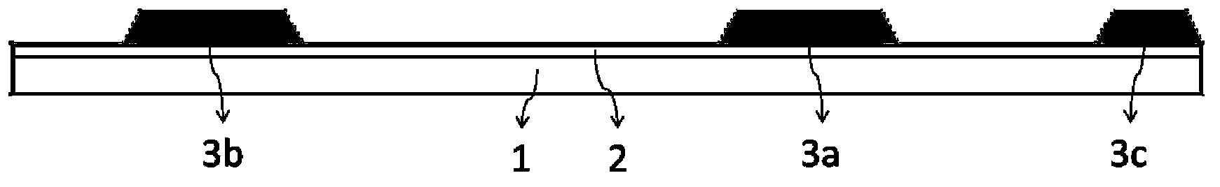
[0129] Such as image 3 shown, in a case with a 50nm thick Si 3 N 4 layer as the buffer layer 2 on the alkali-free glass substrate 1, use PVD to deposit Cu metal film as the grid, the lower electrode of the capacitor and the signal wire, the thickness is 100nm. It is patterned to form the metal layer 3 using a photolithography process. Such as Figure 4 On the patterned gate metal, 100nm of Al was deposited using ALD 2 o 3 as the gate insulating layer 4 . Then PVD is used to deposit metal oxide IGZO (In, Ga, Zn atomic ratio 1:1:1) as the active layer 5 with a thickness of 50 nm. Such as Figure 5 As shown, the Ruihong 304 photoresist 10 is used, and the gate metal pattern is used for self-alignment exposure and development. Such as Figure 14As shown, the active layer 5 is etched using dilute hydrofluoric acid. Then, ALD is used to fabricate Al with a thickness of 50nm 2 o 3 as an etch stop layer 6. The positive photoresist 11 is exposed and developed using a gray...
specific example 3
[0131] Such as image 3 shown, in a SiO with 200nm thick 2 On the non-alkali glass substrate 1 of the buffer layer 2, a Mo metal thin film is deposited by PVD as the gate, the lower electrode of the capacitor and the signal wire, with a thickness of 200nm. It is patterned to form the metal layer 3 using a photolithography process. Such as Figure 4 As shown, on the patterned gate metal, using a combination of PECVD and PVD equipment, under the condition of maintaining a high vacuum, use PECVD to continuously deposit Si with a thickness of 150nm 3 N 4 and 50nm SiO 2 As the gate insulating layer 4, 50 nm of metal oxide IZO (In, Zn atomic ratio 1:1) was deposited as the active layer 5 using PVD. Such as Figure 5 As shown, the Ruihong 304 photoresist 10 is used, and the gate metal pattern is used for self-alignment exposure and development. Such as Figure 6 As indicated, dilute hydrofluoric acid (HF:H 2 O=1:100) to etch the active layer 5, using dry etching equipment, u...
PUM
 Abstract
Description
Claims
Application Information