Method for manufacturing high-growth-rate LED (light-emitting diode) with P-type GaN structure

A technology of growth rate and manufacturing method, applied in electrical components, circuits, semiconductor devices, etc., can solve the problems of poor crystal quality and low luminous efficiency of quantum wells, and achieve the goal of reducing growth time, improving light extraction efficiency, and improving crystal quality. Effect

Inactive Publication Date: 2012-11-07
合肥彩虹蓝光科技有限公司
View PDF8 Cites 18 Cited by
  • Summary
  • Abstract
  • Description
  • Claims
  • Application Information

AI Technical Summary

Problems solved by technology

[0002] At present, in the GaN-based white light diodes produced by the existing technology, the crystal quality of the multi-quantum well (MQW) in the light-emitting layer is not good, resulting in low luminous efficiency of the quantum wells

Method used


Image

  • Method for manufacturing high-growth-rate LED (light-emitting diode) with P-type GaN structure

Examples


Embodiment

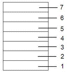
[0020] Such as figure 1 The LED epitaxial structure shown includes: a substrate 1 , a low-temperature GaN buffer layer 2 , a high-temperature GaN buffer layer 3 , an N-type GaN layer 4 , a shallow quantum well 5 , a light-emitting layer multi-quantum well 6 and a p-type GaN layer 7 .

[0021] The specific steps of the manufacturing method of the P-type GaN structure LED with high growth rate are as follows:

[0022] The substrate is annealed in a hydrogen atmosphere, the surface of the substrate is cleaned, the temperature is controlled between 1030-1200°C, and then nitrided. The substrate is a material suitable for the growth of GaN and its semiconductor epitaxial materials, such as Sapphire, GaN single crystal, single crystal silicon, silicon carbide single crystal, etc.;

[0023] Lower the temperature to 500-650°C to grow a low-temperature GaN buffer layer with a thickness of 20-30 nm. During this growth process, the growth pressure is controlled between 300-760 Torr, and ...


PUM

PropertyMeasurementUnit
thicknessaaaaaaaaaa
temperatureaaaaaaaaaa
thicknessaaaaaaaaaa

Abstract

The invention discloses a method for manufacturing a high-growth-rate LED (light-emitting diode) with a P-type GaN structure. The method comprises the following steps of: heating a substrate in a reaction chamber, cooling and growing a low-temperature GaN buffer layer, and heating and growing a high-temperature GaN buffer layer; growing an N-type GaN layer on the buffer layer, growing 2 to 10 InGaN / GaN quantum wells on the N-type GaN layer, and growing 3 to 15 InGaN / GaN quantum wells; and growing a P-type GaN layer on the quantum well layer. The P-type GaN layer is grown by means of a high growth rate, the growth time is shortened, In exertion can be reduced due to the LED structure, and the damage to the InGaN close to the period is reduced; and therefore, the damage to a multiple quantum well structure in a luminous layer is effectively reduced, the quantum well crystal quality is improved, and the light extraction efficiency is improved.

Description

technical field [0001] The invention belongs to the technical field of semiconductors and relates to a method for manufacturing a P-type GaN structure LED, in particular to a method for manufacturing a P-type GaN structure LED with a high growth rate. Background technique [0002] At present, in the GaN-based white light diodes produced by the prior art, the crystal quality of the multiple quantum wells (MQW) in the light-emitting layer is not good, resulting in low luminous efficiency of the quantum wells. Contents of the invention [0003] The purpose of the present invention is to provide a high growth rate P-type GaN structure LED manufacturing method aiming at the above-mentioned shortcomings and deficiencies of the prior art. The invention grows the P-type GaN layer by means of a high growth rate, reduces the growth time, and its LED structure can reduce the volatilization of In, and reduce the damage to InGaN in the adjacent period, thereby effectively reducing the ...

Claims


Application Information

Patent Timeline
Patent Type & Authority Applications(China)
IPC IPC(8): H01L33/00
Inventor 郭丽彬李刚
Owner 合肥彩虹蓝光科技有限公司
Why Eureka
Try Eureka