Deep hole staggered back contact solar battery structure and manufacturing method thereof

A technology of solar cells and manufacturing methods, applied in the direction of final product manufacturing, sustainable manufacturing/processing, circuits, etc., can solve the problems of affecting photoelectric conversion efficiency, large series resistance of batteries, and inability to generate electricity, so as to shorten the diffusion distance, Effect of improving conversion efficiency and reducing recombination loss

Active Publication Date: 2012-11-14
张家口环欧国际新能源科技有限公司
View PDF5 Cites 4 Cited by
  • Summary
  • Abstract
  • Description
  • Claims
  • Application Information

AI Technical Summary

Problems solved by technology

There are two problems with this battery solution. One is that only the carriers that can diffuse to the rear surface can be converted into electrical energy, and those carriers that cannot reach the rear surface due to their short lifespan cannot generate electricity.
The second is that the carriers need to diffuse from the front surface to the back surface, which makes the series resistance of the battery larger and affects the photoelectric conversion efficiency.

Method used


Image

  • Deep hole staggered back contact solar battery structure and manufacturing method thereof
  • Deep hole staggered back contact solar battery structure and manufacturing method thereof
  • Deep hole staggered back contact solar battery structure and manufacturing method thereof

Examples


Embodiment

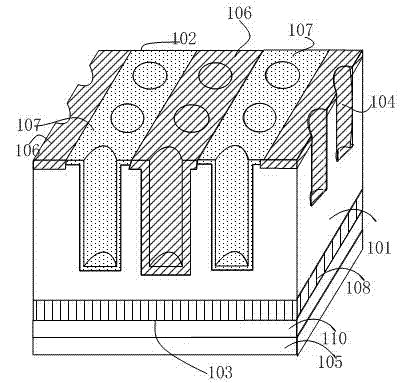
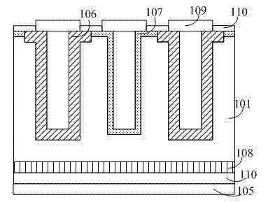
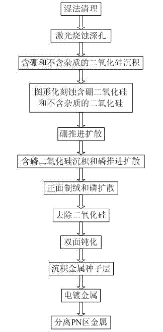
[0022] Example: choose N-type silicon wafers for silicon substrates (P-type monocrystalline silicon wafers and N-type or P-type polycrystalline silicon wafers can also be used), crystal orientation, resistivity 1-20 Ω cm, silicon The slice thickness is 200um, and the deep hole depth is 180um. The specific process steps are as follows (see figure 1 , figure 2 and image 3 ):

[0023] (1) Wet cleaning: the silicon substrate 101 is wet-processed to facilitate the cleaning of the rear surface 102 and the front surface 103 and to etch away rough particles on the surface.

[0024] (2) Laser ablation of deep holes: a laser scanner is used to ablate the rear surface 102 of the silicon substrate 101 to form deep holes 104. The size of the deep holes is related to the thickness of the silicon substrate, and the thickness of the silicon substrate 101) is preferably 200um. The depth of the hole 104 is 180um.

[0025] (3) Boron-containing and impurity-free silicon dioxide deposition...


PUM


Abstract

The invention relates to a photovoltaic device for converting optical energy into electrical energy, and specifically relates to a deep hole staggered back contact solar battery structure and a manufacturing method of the photovoltaic device. By adopting a laser ablation method, deep holes with same depth are respectively formed on the upper surfaces of a P+ type diffusion zone and a N+ type diffusion zone which are formed on the back surface in a staggered manner, wherein the deep holes are not deep enough to reach a doping zone on the front surface of a silicon substrate. The deep holes respectively have same doping concentration and doping depth with the local diffusion zone. According to the invention, by the method of manufacturing the deep holes on a base electrode and an emitting electrode, the problems of failure in effective collection of some short life current carriers and high series resistance cased by long transmission distance of the current carriers in the conventional staggered back electrode scheme are solved. The deep hole structure greatly shortens the diffusion distance of the photon-generated carriers, thus, more photon-generated carriers are collected and the recombination loss of the photon-generated carriers is reduced, the series resistance of batteries is reduced, and the conversion efficiency of the solar battery is further improved.

Description

technical field [0001] The invention relates to a photovoltaic device for converting light energy into electric energy, in particular to a deep-hole staggered back-contact solar cell structure and a manufacturing method thereof. Background technique [0002] At present, one of the most typical solar cell manufacturing methods is to adopt a double-sided electrode scheme, that is, a solar cell manufacturing scheme in which electrodes are drawn from both sides of the silicon wafer on the P-type and N-type doped regions respectively. The feature of this solution is: use a P-type substrate silicon wafer, and do N+ type doping on the surface to form a PN junction. Although the process is simple and the manufacturing cost is low, the conversion efficiency is also low. [0003] In order to improve the conversion efficiency of solar cells, people have proposed a variety of improvement schemes, one of which is the staggered back-contact solar cell manufacturing scheme, which is charac...

Claims


Application Information

Patent Timeline
Patent Type & Authority Applications(China)
IPC IPC(8): H01L31/0352H01L31/0224H01L31/068H01L31/18
CPCH01L31/1804H01L31/03529H01L31/0682Y02E10/547Y02E10/546Y02P70/50
Inventor 王云峰杜春倩郐学良饶祖刚王志刚
Owner 张家口环欧国际新能源科技有限公司
Why Eureka
Try Eureka