Schottky diode and method of formation of Schottky diode

A technology of Schottky diodes and Schottky metals, which is applied in the direction of electrical components, semiconductor/solid-state device manufacturing, circuits, etc., and can solve the problem of narrowing the conduction area, increasing conduction loss, and increasing forward conduction resistance, etc. problems, to achieve the effect of increasing breakdown voltage and increasing thickness

Active Publication Date: 2012-11-21
SHANGHAI HUAHONG GRACE SEMICON MFG CORP
View PDF4 Cites 13 Cited by
  • Summary
  • Abstract
  • Description
  • Claims
  • Application Information

AI Technical Summary

Problems solved by technology

However, when the distance between the two trenches is small, the conduction area becomes narrower, the forward conduction resistance becomes larger, and the conduction loss becomes larger.

Method used


Image

  • Schottky diode and method of formation of Schottky diode
  • Schottky diode and method of formation of Schottky diode
  • Schottky diode and method of formation of Schottky diode

Examples


Embodiment Construction

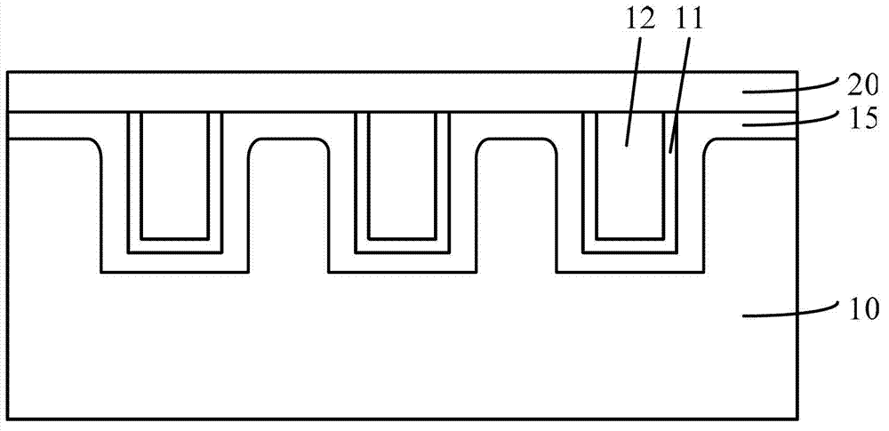
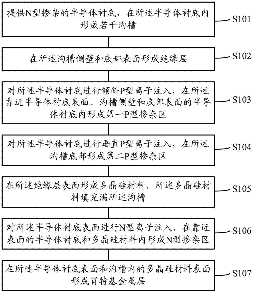
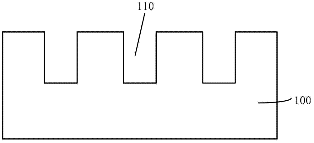
[0033] Since the required distance between adjacent trenches of existing trench Schottky diodes is small, when the distance between the two trenches is small, the conduction from the metal layer to the semiconductor substrate The conduction area becomes narrower, the forward conduction resistance becomes larger, the conduction loss and switching loss become larger, and the forward voltage drop becomes higher. For this reason, the inventor has proposed a Schottky diode and its formation method after research. P-type doped region. When a reverse bias is applied to the Schottky diode subsequently, that is, a positive voltage is applied to the semiconductor substrate, and a negative voltage is applied to the Schottky metal layer, due to the reverse bias, the trench sidewall The thickness of the depletion region between the P-type doped region and the semiconductor substrate is easy to become larger, and the two depletion regions close to the sidewalls of the trench are easy to pi...


PUM


Abstract

The invention discloses a Schottky diode and a method of formation of the Schottky diode. The method of formation of the Schottky diode comprises the following steps: providing a semiconductor substrate and forming a plurality of grooves inside the semiconductor substrate; obliquely injecting P type ions into the semiconductor substrate, and forming first P type doped regions inside the semiconductor substrate close to a surface of the semiconductor substrate, sidewalls of the grooves and a bottom surface; fully filling the grooves with polycrystalline silicon material; inversely forming N type doped regions inside the semiconductor substrate close to the surface and the polycrystalline silicon material; and forming Schottky metal layers on the surface of the semiconductor substrate and the surface of the polycrystalline silicon material. For the spacing between two first P type doped regions of adjacent grooves is less than the spacing between the adjacent grooves, the semiconductor substrate between the two first P type doped regions of the adjacent grooves in the Schottky diode can be cut off by a depletion region more easily when an inverse voltage is applied to two ends of the Schottky diode, so that the inverse breakdown voltage of the Schottky diode can be increased.

Description

technical field [0001] The invention relates to the field of semiconductor manufacturing, in particular to a Schottky diode and a forming method thereof. Background technique [0002] Schottky Barrier Diode (Schottky Barrier Diode) is a low-power, high-current, ultra-high-speed semiconductor device. The metal layer is used as the positive electrode and the semiconductor substrate is used as the negative electrode. The potential barrier formed on the contact surface of the two has rectification characteristics. made. Its reverse recovery time is short (can be as small as a few nanoseconds), the forward voltage is low (0.4 volts), and the rectification current is large (up to several thousand amperes), so it is widely used in switching power supplies, frequency converters, drives, etc. [0003] The U.S. patent document with the publication number US2004 / 0007723A1 discloses a trench Schottky diode. For the specific structure, please refer to figure 1 , including: an N-type do...

Claims


Application Information

Patent Timeline
Patent Type & Authority Applications(China)
IPC IPC(8): H01L21/329H01L29/06H01L29/872
Inventor 苟鸿雁唐树澍
Owner SHANGHAI HUAHONG GRACE SEMICON MFG CORP
Why Eureka
Try Eureka