Manufacturing method for GaN-based LED (Light Emitting Diode) chip for coarsening p-GaN layer nanometer bowl-shaped surface

An LED chip and surface roughening technology, applied in electrical components, circuits, semiconductor devices, etc., can solve the problem of limited light extraction, achieve the effects of low cost, simple process, and increase the probability of extraction

Active Publication Date: 2012-11-21
YANGZHOU ZHONGKE SEMICON LIGHTING
View PDF3 Cites 5 Cited by
  • Summary
  • Abstract
  • Description
  • Claims
  • Application Information

AI Technical Summary

Problems solved by technology

However, there are many problems in the production and removal of the P-GaN rough mask, and the extraction of light is limited

Method used


Image

  • Manufacturing method for GaN-based LED (Light Emitting Diode) chip for coarsening p-GaN layer nanometer bowl-shaped surface
  • Manufacturing method for GaN-based LED (Light Emitting Diode) chip for coarsening p-GaN layer nanometer bowl-shaped surface
  • Manufacturing method for GaN-based LED (Light Emitting Diode) chip for coarsening p-GaN layer nanometer bowl-shaped surface

Examples


Embodiment Construction

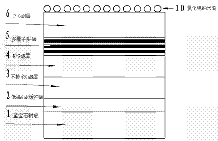
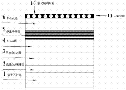
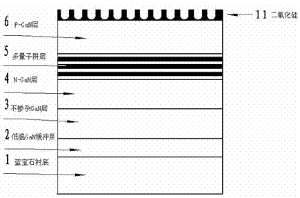
[0027] 1. Preparation of a GaN-based LED chip with p-GaN layer nano-bowl-shaped surface roughening:

[0028] Step 1: Using metal-organic chemical vapor deposition (MOCVD), sequentially grow a 1 μm low-temperature GaN buffer layer 2, a 2 μm undoped GaN layer 3, a 3 μm N-GaN layer 4, and a 200 nm multi-quantum well light-emitting layer on a semiconductor substrate 1 5 and 700nm P-GaN layer 6 to form a GaN epitaxial wafer, wherein the semiconductor substrate 1 is sapphire, silicon, silicon carbide or metal.

[0029] Step 2: put the GaN epitaxial wafer into the evaporation table, vapor-deposit cesium chloride for etching on the surface of the P-GaN layer 6, the time is 5-40min, and the film thickness is 100-800nm;

[0030] Step 3: After the evaporation is completed, fill the chamber of the evaporation table with water vapor for 5 to 20 minutes, so that the cesium chloride on the surface of the P-GaN layer 6 absorbs water and gradually grows to form a cesium chloride nano-islan...


PUM

PropertyMeasurementUnit
etching poweraaaaaaaaaa
diameteraaaaaaaaaa
surface roughnessaaaaaaaaaa

Abstract

The invention provides a manufacturing method for a GaN-based LED (Light Emitting Diode) chip for coarsening a p-GaN layer nanometer bowl-shaped surface and relates to the technical field of photoelectric device production. The manufacturing method comprises the following steps: firstly, evaporating a mask cesium chloride film layer for etching on the surface of a P-GaN layer of a GaN epitaxial wafer; filling water vapor into an evaporating platform chamber, thereby forming a plurality of cesium chloride nanometer islands; depositing silicon dioxide layers on the cesium chloride nanometer islands; soaking or ultrasonically treating the epitaxial wafer in deionized water, thereby forming a silicon dioxide nanometer bowl layer; taking the silicon dioxide nanometer bowl layer as an etching mask; after ending the etching, completely removing the silicon dioxide nanometer bowl layer remained on the GaN epitaxial wafer; performing ICP (Inductively Coupled Plasma) etching on one side of the GaN epitaxial wafer, thereby forming a platform; and evaporating an ITO (Indium Tin Oxide) film on the upper surface of the GaN epitaxial wafer. Compared with the conventional GaN-LED, the GaN-LED after being subjected to surface coarsening has the advantage that the luminous power is increased by above 35%.

Description

technical field [0001] The invention relates to the technical field of photoelectric device production. Background technique [0002] The refractive index of GaN material (n=2.5) is quite different from that of air (n=1), resulting in the critical angle of total reflection at the interface between air and GaN being only 23.6 ° , only a small amount of light generated in the active region escapes outside the material. This requires designing the chip structure to reduce total reflection and increase the critical angle of the escape light cone to improve the light extraction efficiency of the LED chip. [0003] At present, the main technology commonly used at home and abroad is to roughen the surface of P-GaN to increase the surface area of ​​P-GaN and increase the probability of light emission. However, there are many problems in the fabrication and removal of the P-GaN roughening mask, and its effect on light extraction is limited. Contents of the invention [0004] The...

Claims


Application Information

Patent Timeline
Patent Type & Authority Applications(China)
IPC IPC(8): H01L33/22H01L33/00
Inventor 李璟李鸿渐张溢
Owner YANGZHOU ZHONGKE SEMICON LIGHTING
Why Eureka
Try Eureka