Exposure device, exposure and inspection method, and manufacturing method for substrate of display panel

A technology of exposure device and substrate, which is applied to the exposure device of photoengraving process, adopts optical device, measuring device, etc., can solve the problem of beam deformation detection and correction taking a lot of time and effort, and achieves the improvement of drawing accuracy and the suppression of deformation. Effect

Inactive Publication Date: 2012-11-28
HITACHI HIGH-TECH CORP
View PDF8 Cites 6 Cited by
  • Summary
  • Abstract
  • Description
  • Claims
  • Application Information

AI Technical Summary

Problems solved by technology

Therefore, the detection and correction of the beam deformation will take a lot of time and effort

Method used


Image

  • Exposure device, exposure and inspection method, and manufacturing method for substrate of display panel
  • Exposure device, exposure and inspection method, and manufacturing method for substrate of display panel
  • Exposure device, exposure and inspection method, and manufacturing method for substrate of display panel

Examples


Embodiment Construction

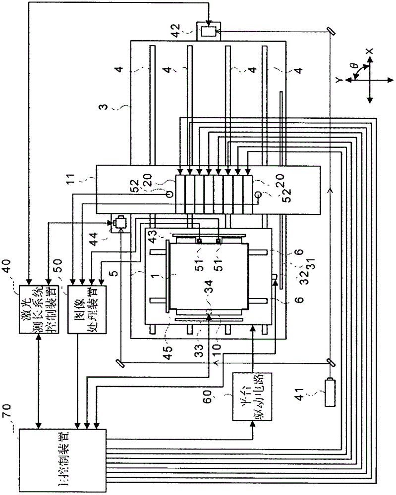
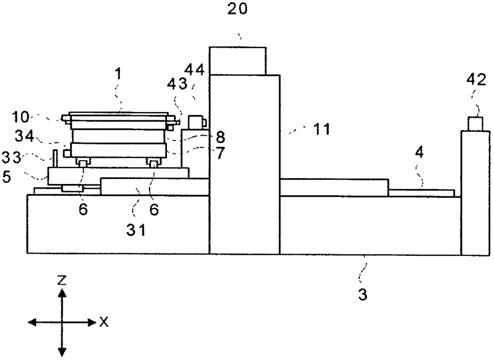
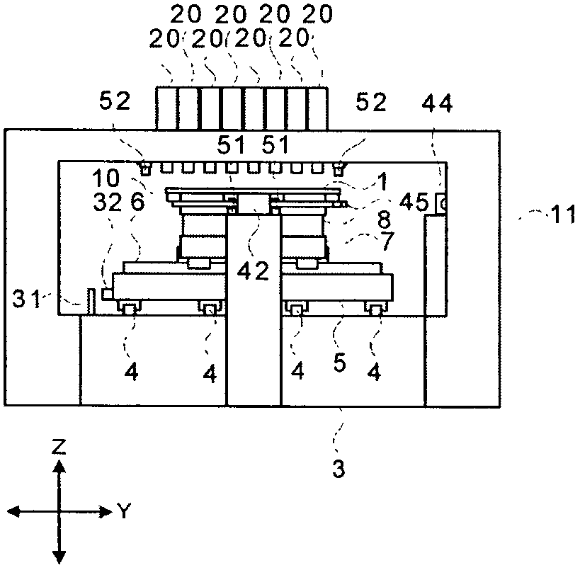
[0068] figure 1 It is a figure which shows the schematic structure of the exposure apparatus which concerns on one Embodiment of this invention. and, figure 2 is a side view of an exposure apparatus according to an embodiment of the present invention, image 3 It is a front view of the exposure apparatus which concerns on one Embodiment of this invention. The exposure device includes a base 3, an X guide 4, an X stage 5, a Y guide 6, a Y stage 7, a θ stage 8, a chuck 10, a gate 11, and a beam irradiation device. 20. Linear scales (linear scale) 31, 33, encoders (encoder) 32, 34, laser length measurement system, laser length measurement system control device 40, image processing device 50, charge coupled device (Charge Coupled Device, CCD) camera (camera) 51, 52, platform drive circuit 60, and main control device 70. In addition, in figure 2 and image 3 In the figure, the laser light source 41 of the laser length measurement system, the laser length measurement system ...


PUM


Abstract

An exposure device, an exposure and inspection method, and a manufacturing method for a substrate of a display panel. The present invention suppresses deformation of a light beam irradiated from a light beam irradiation device, in order to raise a drawing precision. A first image acquisition device (CCD camera (51)) is arranged on a chuck plate, a reticle piece provided with patterns used for inspection is arranged between a head of the light beam irradiation device and the first image acquisition device. Drawing data used for inspection is supplied to a drive circuit of the light beam irradiation device, images of the patterns (2a) used for inspection of the reticle piece and images (2c) of the light beam irradiated from the light beam irradiation device are obtained through the first image acquisition device. Position offset of the light beam is detected from the images of the patterns (2a) used for inspection of the reticle piece and the images (2c) of the light beam obtained by the first image acquisition device, in order to detect deformation of the light beam. Based on a detection result for the deformation of the light beam, coordinates of the drawing data used for exposure are corrected and supplied to the drive circuit of the light beam irradiation device.

Description

technical field [0001] The present invention relates to an exposure device, an exposure method, and a method for manufacturing a display panel substrate using the exposure device and the exposure method. The exposure device is used in the manufacture of a display panel substrate such as a liquid crystal display (display) device. In the method, a light beam is irradiated on a substrate coated with a photoresist, and the substrate is scanned by the light beam to draw a pattern on the substrate. [0002] Furthermore, the present invention relates to an inspection method of an exposure device that irradiates a light beam to a substrate coated with a photoresist, scans the substrate with the light beam, and draws a pattern on the substrate. Background technique [0003] prior art literature [0004] patent documents [0005] Patent Document 1: Japanese Patent Laid-Open No. 2010-44318 [0006] Patent Document 2: Japanese Patent Laid-Open No. 2010-60990 [0007] Patent Document...

Claims


Application Information

Patent Timeline
Patent Type & Authority Applications(China)
IPC IPC(8): G03F7/20G01B11/03
Inventor 林知明吉田稔本田英之
Owner HITACHI HIGH-TECH CORP
Why Eureka
Try Eureka