Method for preparing dielectric film on dual damascene structure through etching forming process

A molding process and dielectric technology, which is applied in the manufacturing of circuits, electrical components, semiconductor/solid-state devices, etc., can solve the problems of increased production costs, complicated processes, and time-consuming operations, so as to reduce equipment loss and optimize production processes. , the effect of improving production efficiency

Inactive Publication Date: 2012-11-28
SHANGHAI HUALI MICROELECTRONICS CORP
View PDF4 Cites 2 Cited by
  • Summary
  • Abstract
  • Description
  • Claims
  • Application Information

AI Technical Summary

Problems solved by technology

[0010] The present invention is aimed at the prior art, the traditional double damascene structure needs to carry out two photolithography processes and three dry etching processes, and after the photoresist coating and etching back process, it is necessary to carry out the necessary steps to improve the pollution level of the wafer. The backside cleaning process of the wafer, the traditional process flow is complicated, the operation is time-consuming, and the production capacity of the semiconductor production process machine is reduced, the efficiency is low, and the cost performance of expensive semiconductor production equipment is low, and the production cost is increased, which limits the development of the semiconductor industry. Development and other defects, providing a method for the etching molding process of the double damascene structure dielectric film

Method used


Image

  • Method for preparing dielectric film on dual damascene structure through etching forming process
  • Method for preparing dielectric film on dual damascene structure through etching forming process
  • Method for preparing dielectric film on dual damascene structure through etching forming process

Examples


Embodiment Construction

[0035] In order to illustrate the technical content, structural features, achieved goals and effects of the present invention in detail, the following will be described in detail in conjunction with the embodiments and accompanying drawings.

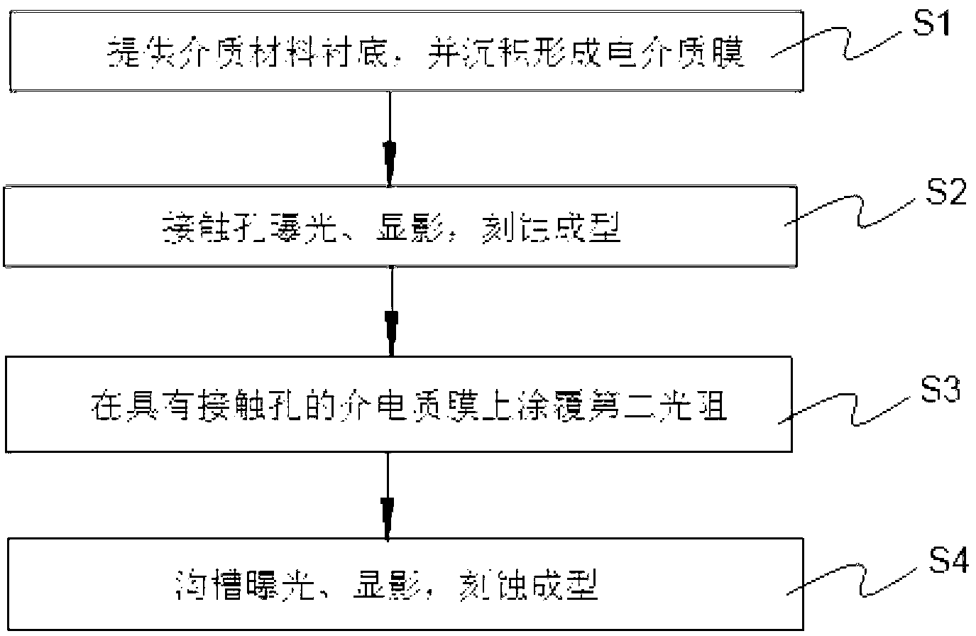
[0036] see figure 1 , figure 1 Shown is the method flow chart of the etching forming process of the double damascene structure dielectric film of the present invention. The method for the etching molding process of the double damascene structure dielectric film comprises the following steps:

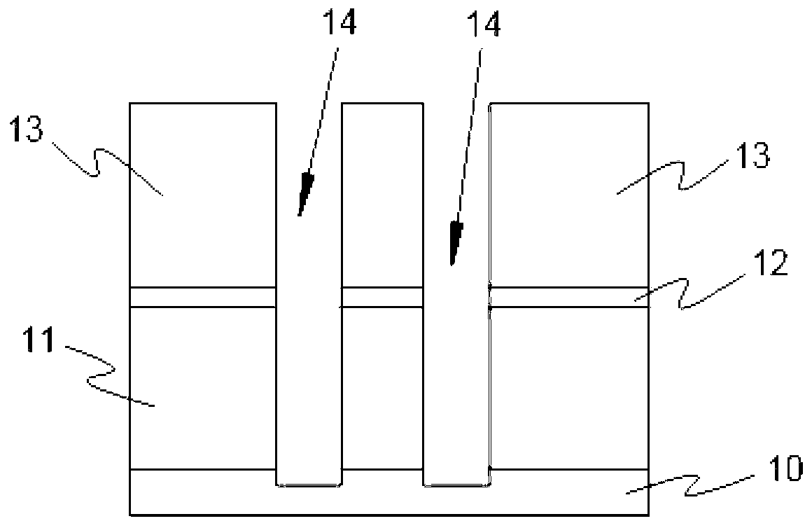
[0037] Executing step S1: providing a dielectric material substrate, and forming the dielectric film on the dielectric material substrate; the dielectric film sequentially includes a low dielectric constant film, Medium buffer layer, overlying layer. In the present invention, preferably, an etching stopper layer is provided between the dielectric material substrate and the low dielectric constant film.

[0038] Executing step S2: exposing, de...


PUM


Abstract

The invention relates to a method for preparing a dielectric film on a dual damascene structure through the etching forming process, which comprises the following execution steps of: (S1) providing a dielectric substrate, and forming a dielectric film on the dielectric substrate; (S2) deeply coating a first photoresist layer different from the surface of the dielectric substrate on an upper overlying layer of the dielectric film, forming the contact hole pattern through exposure and development, and further preparing the contact hole through the etching forming process; (S3) coating a second photoresist layer on the dielectric film with the contact hole; and (S4) coating a third photoresist layer on the second photoresist layer, forming the groove pattern through exposure and development, and preparing the groove through the etching forming process. With the method for preparing a dielectric film on a dual damascene structure through the etching forming process, not only can the production capacity of equipment be increased and equipment loss is reduced, but also the production process is optimized, the production efficiency is increased, and the production cost is lowered.

Description

technical field [0001] The invention relates to the technical field of semiconductor devices, in particular to a method for etching and forming a double damascene structure dielectric film. Background technique [0002] At present, in the copper interconnection process field, the dielectric film etching forming process using a double damascene structure is usually a VFTL (Via First Trench Last, VFTL) process. [0003] Please refer to Figure 6(a), Figure 6(b), Figure 7 , Figure 8 The VFTL process includes three stages of process: [0004] The first stage of process: the first contact hole 2 exposure and development and etching forming process; specifically, on the first etching barrier layer 21, the first dielectric constant film 22, the dielectric buffer layer 23, and the overlying layer 24 , and exposing and developing the photoresist layer 25 to obtain the first contact hole pattern 26 . [0005] The second stage of process: photoresist 3 coating and back etching proc...

Claims


Application Information

Patent Timeline
IPC IPC(8): H01L21/768
Inventor 黄海
Owner SHANGHAI HUALI MICROELECTRONICS CORP
Why Eureka
Try Eureka