Carrier-stored trench gate bipolar transistor

A bipolar transistor, carrier storage technology, applied in semiconductor devices, electrical components, circuits, etc., can solve the problems of increased potential curvature radius, electric field concentration, device breakdown, etc., to achieve low power consumption, high withstand voltage , the effect of improving the turn-off speed

Inactive Publication Date: 2012-11-28
UNIV OF ELECTRONICS SCI & TECH OF CHINA +1
View PDF3 Cites 13 Cited by
  • Summary
  • Abstract
  • Description
  • Claims
  • Application Information

AI Technical Summary

Problems solved by technology

However, due to the addition of the CS layer, the potential curvature radius at the edge of the groove gate will increase significantly, which will lead to the occurrence of electric field concentration there, and the device is prone to premature breakdown at the edge of the groove gate.

Method used


Image

  • Carrier-stored trench gate bipolar transistor
  • Carrier-stored trench gate bipolar transistor
  • Carrier-stored trench gate bipolar transistor

Examples


Embodiment Construction

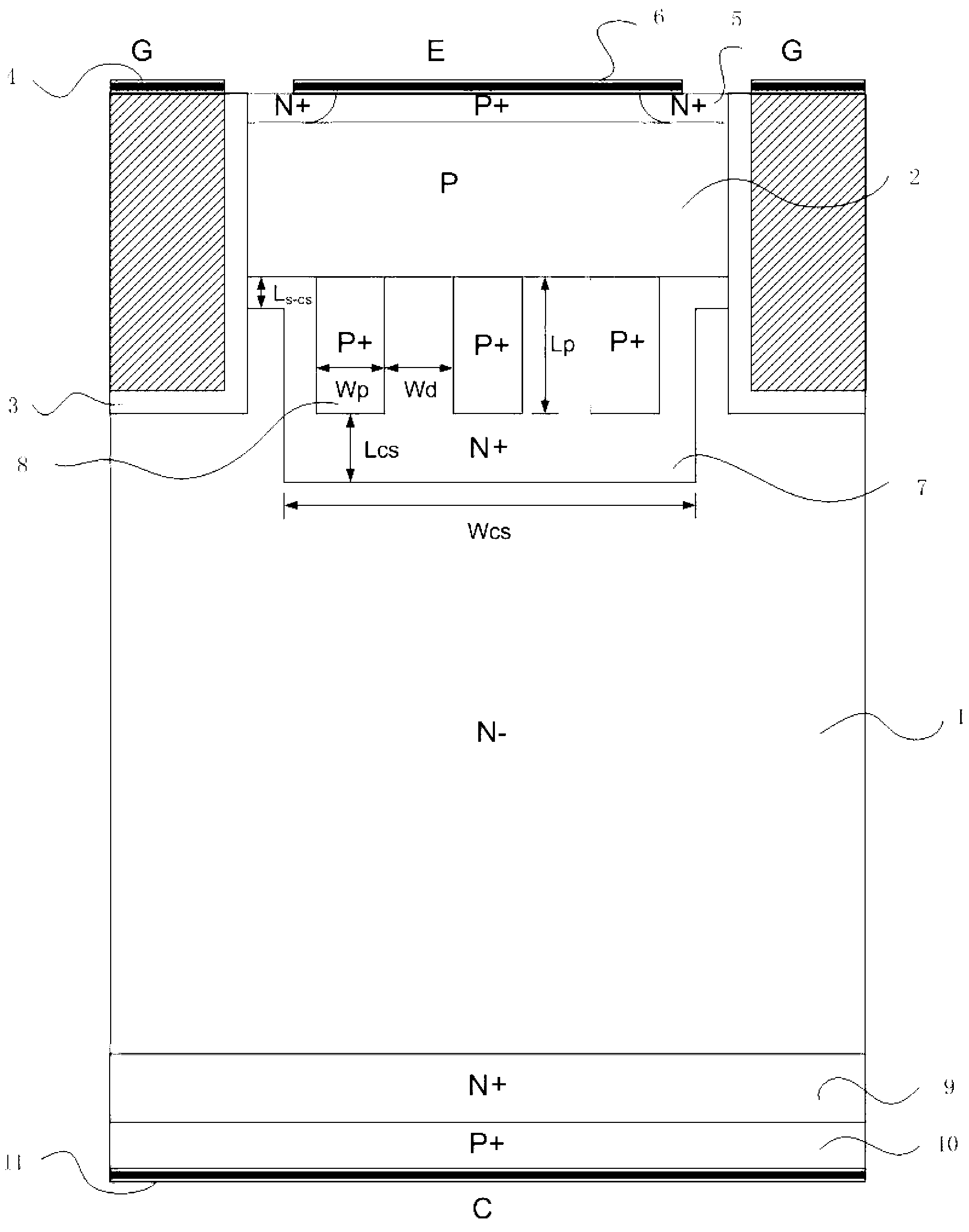
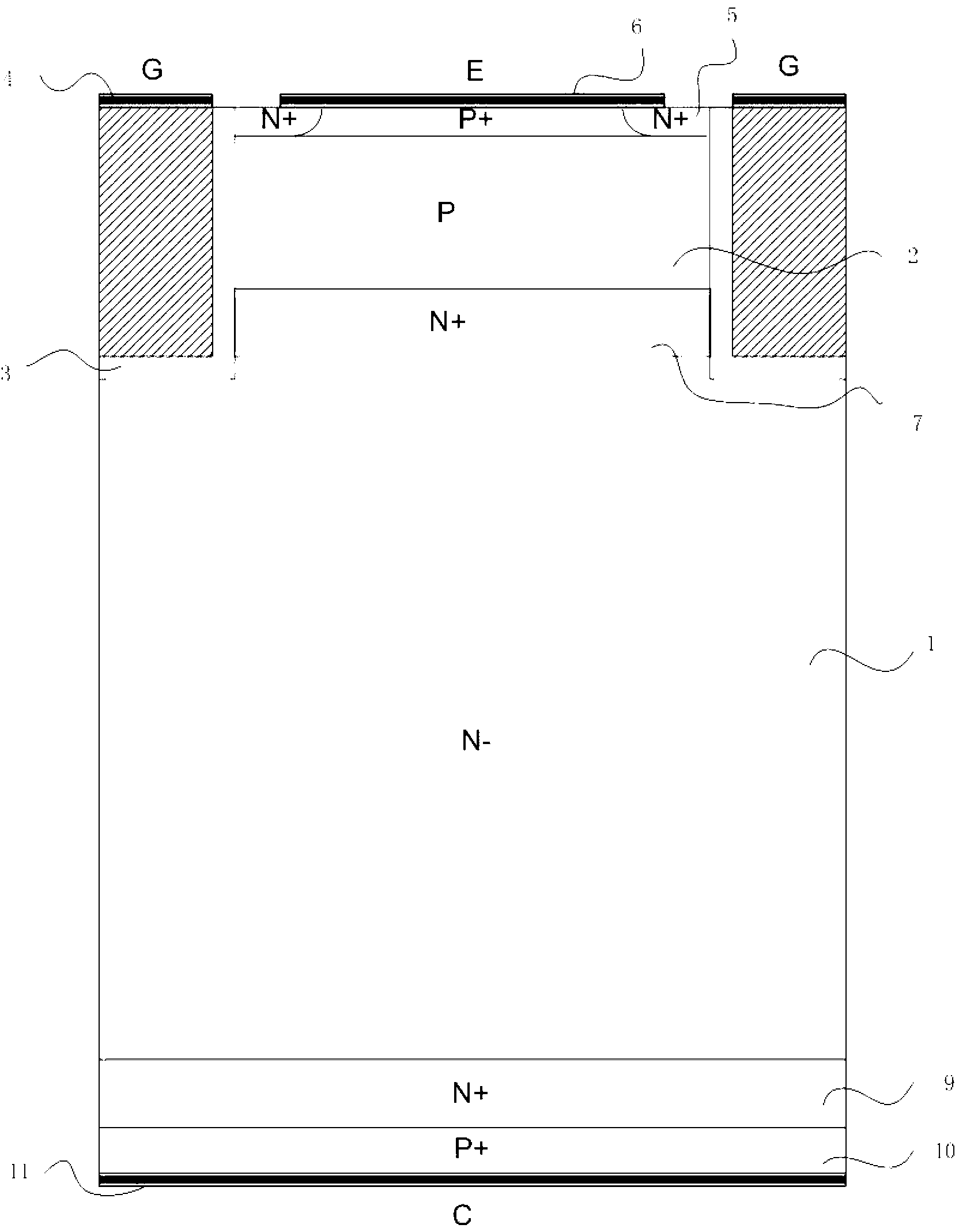
[0019] A carrier storage tank gate bipolar transistor, such as figure 1 As shown, it includes a collector structure, a drift region structure, an emitter structure and a gate structure; the collector structure includes a P+ collector region 10 and a metallized collector 11 on the back of the P+ collector region 10; the drift region structure Including the N-layer 1 located on the front of the P+ collector region 10; the gate structure is a trench gate structure, located on both sides of the top layer of the N-layer 1, formed by trench type polysilicon gate, metallization of the surface of the trench type polysilicon gate The gate 4 and the gate oxide layer 3 on the sides and bottom of the trench polysilicon gate; The P+ contact region in the middle of the top of the region 2, the metallized emitter 6 in contact with the surface of the N+ emitter region 5 and the P+ contact region, and the N+ carrier storage layer 7 between the P-type base region 2 and the N-layer 1; The side...


PUM


Abstract

The invention provides a carrier-stored trench gate bipolar transistor (FMP-CSTBT), and belongs to the technical field of power semiconductor devices. According to the carrier-stored trench gate bipolar transistor, a plurality of P+ strips are inserted into an N+ carrier stored layer under a P type base area of a common CSTBT, wherein the top surface of a P+ strip 8 is in contact with a P type base area 2, and while the bottom surfaces are in contact with an N- layer 1; and the length direction of the P+ strip 8 is parallel to the width direction of the whole device. The P+ strips are partially depleted to generate negative depletion charges when the device is subject to pressure resistance, so that an electric field close to the edge of a trench gate can be modulated, the radius of curvature of the potential in the edge of the trench gate can be reduced, and as a result, the peak value of the electric field is transferred to a PN node of the base area, therefore, the device is prevented form being punctured in advance, and the reverse pressure resistance and the stability of the device can be effectively improved. The P type strips without being completely depleted provide additional extracting channels for conveying fewer carriers, so as to accelerate the extraction, shorten the turn-off time and reduce the turn-off loss.

Description

technical field [0001] The invention belongs to the technical field of power semiconductor devices, and relates to a carrier stored trench bipolar transistor (Carrier Stored Trench Bipolar Transisitor, CSTBT for short). Background technique [0002] High-voltage power semiconductor devices are an important part of power electronics, and have a wide range of applications in fields such as motor drives in power systems and frequency conversion in consumer electronics. In applications, high-voltage power semiconductor devices need to have characteristics such as low conduction power consumption, large conduction current, high voltage blocking capability, simple gate drive, and low switching loss. Insulated Gate Bipolar Transistor (IGBT for short) is widely used due to its superior performance in the field of medium and high voltage power electronics. However, as a bipolar device, the IGBT has a trade-off relationship between its key parameters, the turn-on voltage drop and the...

Claims


Application Information

Patent Timeline
Patent Type & Authority Applications(China)
IPC IPC(8): H01L29/10H01L29/739
Inventor 陈万军齐跃汪志刚张波李泽宏
Owner UNIV OF ELECTRONICS SCI & TECH OF CHINA
Why Eureka
Try Eureka