Light-emitting diode surface metal sub-wavelength embedded grating structure and method for preparing same

A light-emitting diode and grating structure technology, which is applied in the direction of electrical components, circuits, semiconductor devices, etc., can solve the problems that the P-type layer cannot be grown continuously, and the distance cannot be satisfied, so as to improve the spontaneous emission rate, reduce the divergence angle of the outgoing light, Effect of improving internal quantum efficiency

Inactive Publication Date: 2012-11-28
UNIV OF ELECTRONICS SCI & TECH OF CHINA
View PDF5 Cites 14 Cited by
  • Summary
  • Abstract
  • Description
  • Claims
  • Application Information

AI Technical Summary

Problems solved by technology

However, there will be obstacles in the actual production process of LED chips: first of all, for the MOCVD method widely used in the production of LED chips, it is impossible to directly make nano-metal bodies on the light-emitting layer, because the metal layer cannot continue. Growth of P-type layer; in order to ensure the lateral diffusion of current, the thickness of P-type layer is often greater than 300nm
Therefore, if the nano-metal body is placed on the surface and the isolation layer is added, the distance between the nano-metal body and the light-emitting layer cannot meet the above requirements.

Method used


Image

  • Light-emitting diode surface metal sub-wavelength embedded grating structure and method for preparing same
  • Light-emitting diode surface metal sub-wavelength embedded grating structure and method for preparing same
  • Light-emitting diode surface metal sub-wavelength embedded grating structure and method for preparing same

Examples


Embodiment Construction

[0024] The present invention will be further described below in conjunction with the accompanying drawings and specific embodiments.

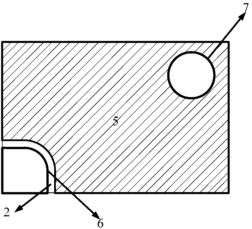
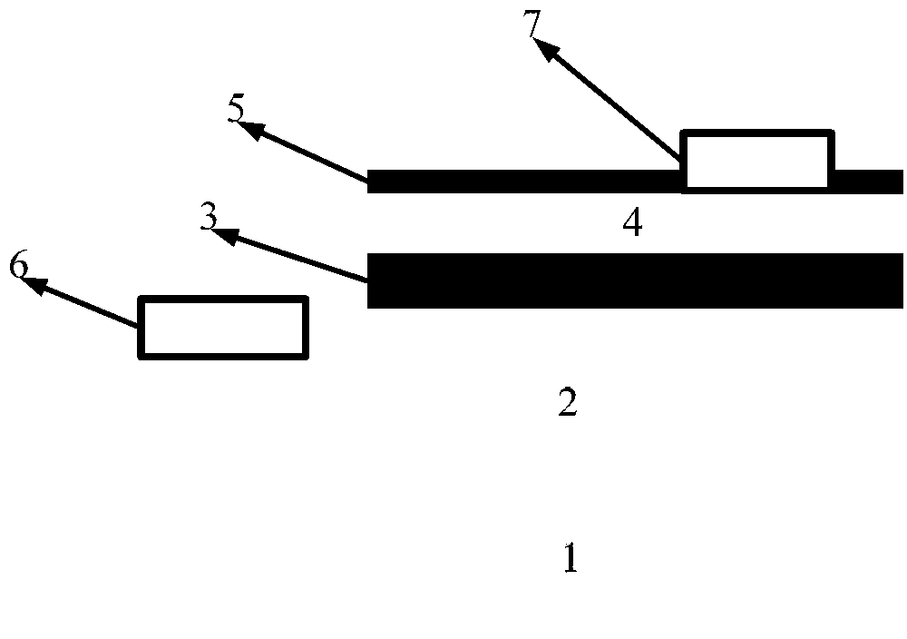
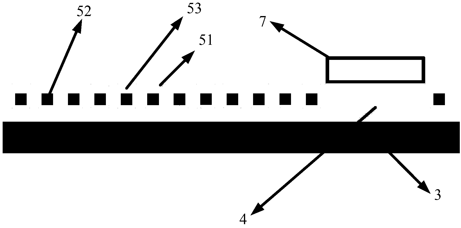
[0025] Such as Figure 1A and Figure 1B In the LED chip structure shown, a substrate 1 , an n-type layer 2 , a light-emitting layer 3 and a p-type layer 4 are sequentially stacked on the substrate 1 from bottom to top. The substrate 1 can be made of sapphire; the n-type layer 2 and the p-type layer 4 can be a multilayer structure according to specific requirements, for example, the n-type layer 2 can include a buffer layer, an electron injection layer, an electron transport layer, a hole blocking layer, etc. The light-emitting layer 3 can usually also be a multilayer structure, such as a multi-quantum well structure, etc.; the n-type layer 2 is provided with an n-electrode 6 , and the p-type layer 4 is provided with a p-electrode 7 . The structure of the above-mentioned LED chip is a prior art, so it will not be described in detail.

[0026]...


PUM

PropertyMeasurementUnit
thicknessaaaaaaaaaa
thicknessaaaaaaaaaa
thicknessaaaaaaaaaa

Abstract

The invention relates to a light-emitting diode surface metal sub-wavelength embedded grating structure and a method for preparing the same. The light-emitting diode surface metal sub-wavelength embedded grating structure is positioned above a p-type layer which comprises a substrate, an n-type layer, a light-emitting layer and a light-emitting diode (LED) chip of the p-type layer. The light-emitting diode surface metal sub-wavelength embedded grating structure is characterized by comprising an isolating layer, a nanometallic body and a protection layer, wherein the isolating layer is embedded in a concave groove which is periodically distributed on the upper surface of the p-type layer, and is used for preventing energy which is coupled to surface plasmon polaritons (SPPs) from being lost due to the ohmic contact existing between the nanometallic body and the p-type layer; the nanometallic body is embedded into the isolating layer, and adopts metal, the thickness of the isolating layer is 50-100 nanometers, and the depth of the concave groove of the p-type layer is determined according to the thickness of the p-type layer; and the protection layer is arranged on the nanometallic body. The light-emitting diode surface metal sub-wavelength embedded grating structure has the beneficial effects that the spontaneous radiation rate of coupled SPPs and light-emitting layers of multiple quantum wells is greatly improved, and furthermore, the internal quantum efficiency is greatly improved.

Description

technical field [0001] The invention belongs to the technical field of light-emitting diodes (LEDs), in particular to the field of light-emitting diodes (LEDs) enhanced by surface plasmons (SPPs, Surface Plasmon Polaritons) excited by metal subwavelength embedded gratings. Background technique [0002] SPPs are electromagnetic wave patterns caused by the interaction of light and free electrons on metal surfaces. It is confined near the metal-dielectric interface, propagates along the surface, and decays exponentially in the direction perpendicular to the interface. Its electromagnetic energy is strongly bound near the interface and has a strong near-field enhancement effect. SPPs have a higher wavenumber than light propagating in air, so they are currently widely used in near-field light applications and nanophotonics, but at the same time, SPPs cannot be directly coupled with light waves. Therefore, it is necessary to add a special structure at the interface between the me...

Claims


Application Information

Patent Timeline
Patent Type & Authority Applications(China)
IPC IPC(8): H01L33/20H01L33/04H01L33/00
Inventor 林祖伦宋科田祁康成曹贵川
Owner UNIV OF ELECTRONICS SCI & TECH OF CHINA
Why Eureka
Try Eureka