Super-junction vertical double-diffusion metal-oxide-semiconductor (VDMOS) device with dynamic charge balance

A charge balancing and dynamic technology, applied in electrical components, semiconductor devices, circuits, etc., can solve the problems of limiting the forward safe working area of ​​the device, device temperature rise, device failure, etc., to expand the forward safe working area, alleviate the charge Unbalance, the effect of increasing the current range

Inactive Publication Date: 2012-12-05
UNIV OF ELECTRONICS SCI & TECH OF CHINA +1
View PDF3 Cites 3 Cited by
  • Summary
  • Abstract
  • Description
  • Claims
  • Application Information

AI Technical Summary

Problems solved by technology

The instantaneous additional carriers introduced by the large current break the charge balance between the p-column region and the n-column region, change the electric field distribution of the withstand voltage layer, and reduce the avalanche breakdown voltage of the device. The large avalanche current that appears in advance will cause the device Temperature rise triggers parasitic effects in the device, causing secondary breakdown and device failure
And the larger the current, the more prone to avalanche breakdown of the device, which limits the forward safe working area of ​​the device

Method used


Image

  • Super-junction vertical double-diffusion metal-oxide-semiconductor (VDMOS) device with dynamic charge balance
  • Super-junction vertical double-diffusion metal-oxide-semiconductor (VDMOS) device with dynamic charge balance
  • Super-junction vertical double-diffusion metal-oxide-semiconductor (VDMOS) device with dynamic charge balance

Examples


Embodiment Construction

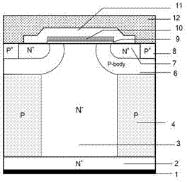
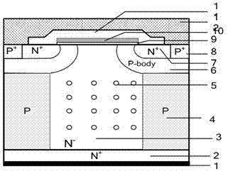
[0024] A super junction VDMOS device with dynamic charge balance, its structure is as figure 2 Shown, including N + Substrate 2, located at N + The metalized drain electrode 1 on the back of the substrate 2 is located at N + The super junction structure on the front side of the substrate 2; the super junction structure consists of N - The epitaxial region 3 and the P-type pillar region 4 are formed alternately; there is a P-type base region 6 on both sides of the top of the super junction structure, and the P-type base region 6 is connected to the N - The epitaxial region 3 is in contact with the P-type pillar region 4; each P-type base region 6 has an N + Source area 7 and a P + Body area 8, N + Source area 7 and P + The two body regions 8 are in contact with the metalized source electrode 12; the gate oxide layer 9 covers the two P-type base regions 6 and the N between them. - On the surface of the epitaxial region 3, the upper surface of the gate oxide layer 9 is a polysilicon ...


PUM


Abstract

The invention discloses a super-junction vertical double-diffusion metal-oxide-semiconductor (VDMOS) device with dynamic charge balance and belongs to the field of power semiconductor devices. Deep-energy level impurities (for an N-channel device, a main impurity S, Se or Te; and for a P-channel device, a main impurity In, Ti or Zn) is doped into an epitaxial region (3) of a super junction structure of the conventional super junction VDMOS device. Ionization rates of the deep-energy level impurities are low at room temperature, and the contribution to the dosage concentration of a super-junction center pillar column (4) can be neglected, so that static charge balance of the device is not influenced; when the device is switched in the forward direction and operated under high current, the ionization rates of the deep-energy level impurities are greatly improved along with the raise of the temperature of the device, and equivalently, the doping level of the epitaxial region (3) is improved, so that a phenomenon that avalanche breakdown voltage of the device is dropped caused by the charge unbalance of the super-junction structure when a charge carrier flows by the epitaxial region (3) is avoided; and therefore, the operative current range of the device is widened, and a forward direction safe operation zone of the device is enlarged.

Description

technical field [0001] The invention belongs to the technical field of power semiconductor devices, and relates to a vertical double-diffused metal oxide semiconductor device (VDMOS device), especially a VDMOS device with a super junction structure (Super Junction). Background technique [0002] At present, the application fields of power semiconductor devices are becoming wider and wider, and can be widely used in DC-DC converters, DC-AC converters, relays, motor drives and other fields. Compared with bipolar transistors, vertical double-diffused metal-oxide-semiconductor field-effect transistors (VDMOS) have the advantages of fast switching speed, low loss, high input impedance, low driving power, good frequency characteristics, and highly linear transconductance. The most widely used new power device at present. However, conventional VDMOS devices also have their inherent disadvantages, that is, the on-resistance increases with the withstand voltage (R on ∝BV 2.5 ) res...

Claims


Application Information

Patent Timeline
Patent Type & Authority Applications(China)
IPC IPC(8): H01L29/78H01L29/06
Inventor 任敏赵起越邓光敏李巍张蒙张灵霞李泽宏张金平张波
Owner UNIV OF ELECTRONICS SCI & TECH OF CHINA
Why Eureka
Try Eureka