Method for manufacturing distributed feedback laser device array by virtue of selection region epitaxy technology

A technology of selective area epitaxy and laser array, applied in the direction of lasers, laser devices, semiconductor lasers, etc., can solve the problems of thickness material quality degradation, effective refractive index change, deviation from gain peak, etc.

Active Publication Date: 2014-02-12
INST OF SEMICONDUCTORS - CHINESE ACAD OF SCI
View PDF2 Cites 1 Cited by
  • Summary
  • Abstract
  • Description
  • Claims
  • Application Information

AI Technical Summary

Problems solved by technology

The disadvantage of this scheme is that while the effective refractive index of the material changes with the thickness, the emission wavelength of the quantum well also changes with the thickness of the material.
Since the emission wavelength of the quantum well material is very sensitive to the thickness of the quantum well, as the thickness of the material changes, the change speed of the quantum well emission wavelength is much faster than the change speed of the Bragg wavelength of the distributed feedback laser, which will cause the Bragg wavelength of some array units to deviate from the quantum Gain peaking of the well material, leading to deterioration of its single-mode characteristics
In addition, because quantum well materials generally have a large strain, a significant increase in thickness will lead to a significant decrease in material quality

Method used


Image

  • Method for manufacturing distributed feedback laser device array by virtue of selection region epitaxy technology
  • Method for manufacturing distributed feedback laser device array by virtue of selection region epitaxy technology
  • Method for manufacturing distributed feedback laser device array by virtue of selection region epitaxy technology

Examples


no. 1 example

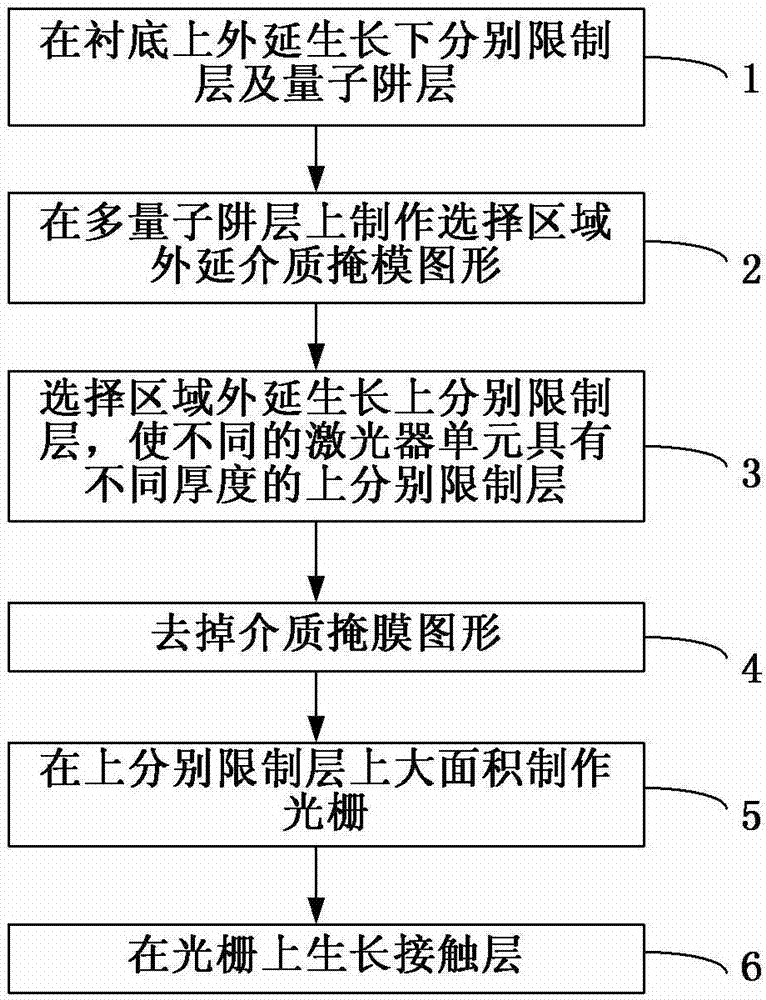
[0031] see figure 1 , image 3 , Figure 5 and Image 6 As shown, the present invention provides a method (first embodiment) for making a distributed feedback laser array using the selective area epitaxy technique, comprising the following steps:

[0032] Step 1: Epitaxially grow the confinement layer 2 and the quantum well layer 3 respectively on the substrate 1. The substrate 1 is a GaAs substrate, InP substrate, GaN substrate, SiC substrate, Si substrate, or other III-V , II-VI group material substrate;

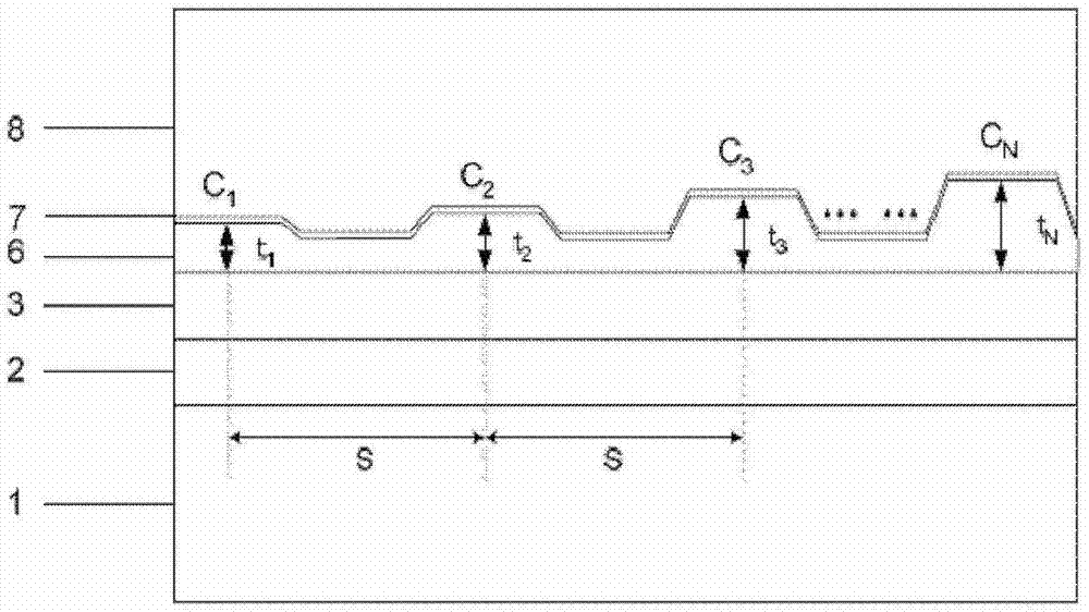
[0033] Step 2: making a selective area epitaxial dielectric mask pattern 4 on the quantum well layer 3 ( Figure 5 ) or 5( Image 6 ). The period of the dielectric mask pair in mask pattern 4 or 5 and the period of the array unit ( image 3 ) are the same, both are S. mask pattern 4 ( Figure 5 ) The distance between the mask pairs remains unchanged, and the mask width gradually increases, that is, the mask M 1 , M 2 , M 3 to M N The width satisfies W 1 2 3 N...

no. 2 example

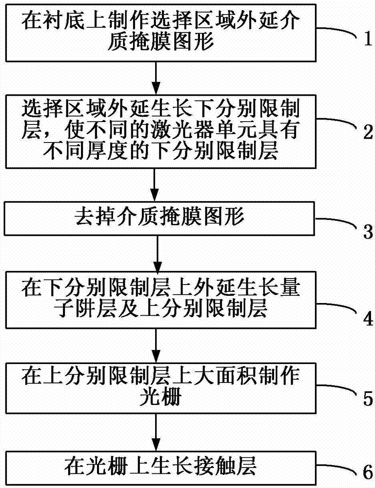
[0038] see again figure 2 , Figure 4 , Figure 5 and Image 6 As shown, the present invention also provides a method (second embodiment) for making a distributed feedback laser array using the selective area epitaxy technique, comprising the following steps:

[0039] Step 1: making a selective area epitaxial dielectric mask pattern 4 on the substrate 1 ( Figure 5 ) or 5( Image 6 ). The substrate 1 is a GaAs substrate, an InP substrate, a GaN substrate, a SiC substrate, a Si substrate, or other III-V, II-VI group material substrates. The period of the dielectric mask pair in mask pattern 4 or 5 and the period of the array unit ( Figure 4 ) are the same, both are S. mask pattern 4 ( Figure 5 ) The distance between the mask pairs remains unchanged, and the mask width gradually increases, that is, the mask M 1 , M 2 , M 3 to M N The width satisfies W 1 2 3 N . mask pattern 5( Image 6 ) in which the mask width remains constant and the mask pair spacing gradual...


PUM


Abstract

A method for manufacturing a distributed feedback laser array includes: forming a bottom separate confinement layer on a substrate; forming a quantum-well layer on the bottom separate confinement layer; forming a selective-area epitaxial dielectric mask pattern on the quantum-well layer; forming a top separate confinement layer on the quantum-well layer through selective-area epitaxial growth using the selective-area epitaxial dielectric mask pattern, the top separate confinement layer having different thicknesses for different laser units; removing the selective-area epitaxial dielectric mask pattern; forming an optical grating on the top separate confinement layer; and growing a contact layer on the optical grating. The present disclosure achieves different emission wavelengths for different laser units without significantly affect emission performance of the quantum-well material.

Description

technical field [0001] The invention relates to the field of optoelectronic devices, in particular to a method for manufacturing a distributed feedback laser array by using a selective area epitaxy technique. Background technique [0002] Multiwavelength lasers are the core devices of modern wavelength division multiplexing (WDM) optical communication systems. Due to the advantages of compact structure, low optical and electrical connection loss, high stability and reliability, monolithically integrated multi-wavelength laser arrays have broad application prospects in WDM systems. At present, a variety of manufacturing methods for monolithic integrated multi-wavelength laser arrays have been developed, including the use of electron beam exposure technology, multi-step holographic exposure technology, sampling grating technology, and selective area epitaxy technology. [0003] Among the above technologies, the use of selective area epitaxy (SAG) technology to fabricate monol...

Claims


Application Information

Patent Timeline
Patent Type & Authority Patents(China)
IPC IPC(8): H01S5/40H01S5/30H01S5/12
CPCH01S5/12H01S5/4087H01S5/2077H01S5/3407
Inventor 梁松张灿朱洪亮王圩
Owner INST OF SEMICONDUCTORS - CHINESE ACAD OF SCI
Why Eureka
Try Eureka