
Circuit layout structure for detecting dishing on copper interconnect lines

A technology of layout structure and interconnection line, applied in material capacitance, electromagnetic measurement device, electric/magnetic depth measurement, etc., can solve the problems of general lateral resolution, complicated operation, wafer surface damage, etc. The experimental measurement is convenient to verify the effect of uniformity

Inactive Publication Date: 2015-08-19
HEBEI UNIV OF TECH
View PDF2 Cites 0 Cited by
  • Summary
  • Abstract
  • Description
  • Claims
  • Application Information

AI Technical Summary

Problems solved by technology

The effect of surface topography measurement is intuitive and reliable, but due to the limitations of the testing equipment used, there are still many limitations and deficiencies
The surface profiler based on the optical principle has a fast scanning speed and can obtain the three-dimensional topography of a large area of ​​the wafer surface in a short time, but its horizontal and vertical resolution is low, and it is gradually unsuitable for the process node below 90nm Copper interconnection CMP detection; the surface profiler based on the mechanical contact principle currently has a high vertical resolution, but the horizontal resolution is average, the scanning speed is slow, and it is easy to cause damage to the wafer surface; the atomic force microscope has little damage to the sample surface, and the resolution The detection rate is high, but the detection range is extremely limited. Usually, the reliable scanning area is only within tens of microns. At present, 300mm and 480mm have become the mainstream standard of silicon wafer size. The AFM detection is not only cumbersome to operate, but also complicated and inefficient.

Method used


Image

  • Circuit layout structure for detecting dishing on copper interconnect lines

Examples


Embodiment 1

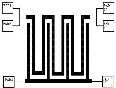
[0012] Example 1: The copper wire of the bending structure is a four-terminal structure, and its resistance value can be accurately measured by the Kelvin method; at the same time, PAD1, PAD1', PAD2, and PAD2' are placed at low or high levels, When PAD3 and PAD3' are placed at opposite levels, the capacitance value of the comb structure can be measured.

[0013] Comb-tooth structure capacitance value measured by The groove depth of the copper wire can be calculated according to formula (1), where represents the groove depth, is the vacuum permittivity, is the dielectric constant of the low-K medium, is the distance between the Cu meander line and the Cu comb line, is the length of the Cu meander.

[0014] Formula 1)

[0015] Therefore, the resistance value of the copper meandering wire can be further calculated by formula (2), where Indicates the copper meander resistance, is the resistivity of Cu, is the length of the Cu meander, is the wi...


PUM


Abstract

The invention discloses a circuit layout structure for detecting whether a saucer pit is produced by a copper interconnection line. The layout structure comprises a copper line of a bent structure and a copper line provided with comb teeth, wherein the comb teeth are arranged in a bent space; the two ends of the copper line of the bent structure are provided with two input end heads or output end heads respectively; and the two ends of the copper line provided with the comb teeth are provided with the input or output end heads respectively. Measurement can be performed by using the structure provided by the invention without being affected by the size of the line, an entire chip can be conveniently measured, and the uniformity of the chip CMP (Chemical Mechanical Polishing) is verified excellently.

Description

technical field [0001] The invention relates to the field of electrical measurement structure for detecting and evaluating the global planarization process of multilayer metal wiring, more specifically, relates to a circuit layout structure for detecting whether dish-shaped pits are generated in copper interconnection lines during chemical mechanical polishing. Background technique [0002] The current ultra-large-scale integrated circuit (ULSI) manufacturing has entered the ultra-deep sub-micron process stage. With the reduction of device size and the increase of operating frequency, interconnection delay and crosstalk have become the bottleneck restricting the performance of the entire circuit. From 0.13μm to 45nm and below technology nodes, integrated circuit interconnection adopts copper (Cu) interconnection and low dielectric constant (Low-K) dielectric technology to reduce the impact of various parasitic effects on circuit performance; at the same time, in order to o...

Claims


Application Information

Patent Timeline
Patent Type & Authority Patents(China)
IPC IPC(8): G01N27/20G01N27/24G01B7/26
Inventor 王伟刘玉岭潘国峰王如王胜利
Owner HEBEI UNIV OF TECH
Learn More