OLED device with improved light extraction rate through ps microsphere layer and its manufacturing method

A manufacturing method and microsphere layer technology, which is applied in semiconductor/solid-state device manufacturing, electrical solid-state devices, semiconductor devices, etc., can solve problems such as blurred image display, complicated process, and low reliability, and achieve lumen efficiency improvement and chemical stability Good sex, not easy to fall off

Inactive Publication Date: 2015-12-02
SOUTH CHINA UNIV OF TECH
View PDF3 Cites 0 Cited by
  • Summary
  • Abstract
  • Description
  • Claims
  • Application Information

AI Technical Summary

Problems solved by technology

[0005] For the first solution, roughening the light-emitting surface directly, although the process is simple, is likely to cause damage to the device, and the uncertainty of the roughening is likely to lead to poor uniformity of the photoelectric performance of the device
For the second scheme, the basic manufacturing method is to deposit a specific thickness of MgF on the light-emitting surface of the OLED. 2 Membrane, using MgF 2 The characteristic of the refractive index of 1.38 plays the role of the refractive index matching layer, thereby improving the light output; however, the light output rate that can be improved by this structural design is not high, and it is necessary to vacuum-deposit a new layer of material on the outer surface of the OLED. In the evaporation device, The organic polymer properties of each functional layer in the OLED will inevitably be affected, making the performance of the light-emitting device unstable and low in reliability. At the same time, this design scheme also has the disadvantages of complex process and high cost, which is not conducive to industrial mass production.
For the third scheme, a large number of microlenses with a size of tens of microns are arranged in a plane matrix on the microlens film, and the microlenses arranged in a plane matrix scatter light. This method has the following problems. It is a regular array of micro-lens matrix, the scattering of light is uneven, the scattering effect is very poor, it is easy to cause the light output of the light-emitting device to be blurred, and the displayed image is very blurred. Large-scale industrial production is difficult and costly
It can be seen that the existing technology mainly has the following defects: (1) the light output effect is not ideal, which will cause damage to the structure or performance of the OLED itself; (2) it is difficult to realize mass production, the process is complicated, and the cost is high; The scattering effect is poor, and the image display is blurred; (4) The performance of the light-emitting device is unstable and the reliability is low

Method used


Image

  • OLED device with improved light extraction rate through ps microsphere layer and its manufacturing method
  • OLED device with improved light extraction rate through ps microsphere layer and its manufacturing method
  • OLED device with improved light extraction rate through ps microsphere layer and its manufacturing method

Examples


Embodiment

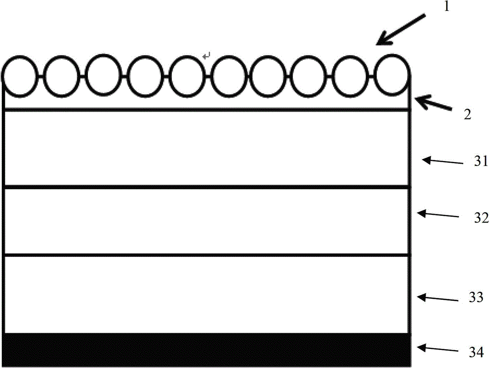
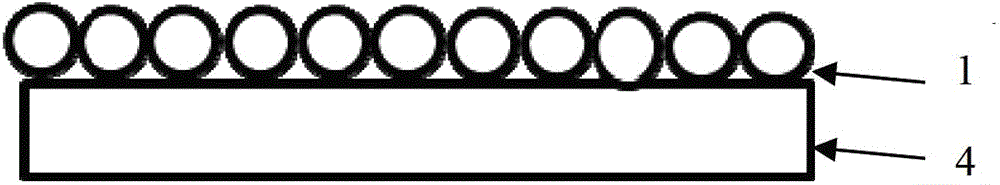
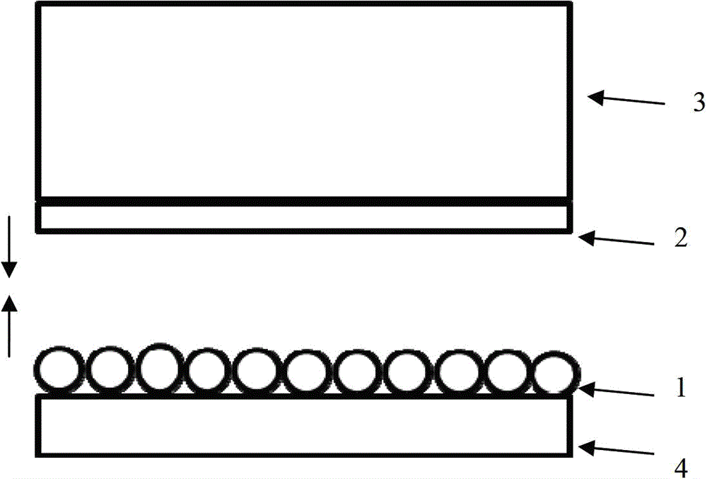
[0053] Such as figure 1 As shown, the OLED device in this embodiment that improves the light extraction rate through the PS microsphere layer includes an OLED element 3, a PDMS film 2 disposed on the light-emitting surface of the OLED element, and one side of the PDMS film 2 is attached to the light-emitting surface of the OLED element 3. The other side is provided with a PS microsphere layer 1 . The PS microsphere layer 1 is composed of a single layer of PS microspheres, that is, the thickness of the PS microsphere layer 1 is the diameter length of the PS microspheres.

[0054] The OLED element is a bottom emission OLED element 3, including a glass substrate layer 31, an ITO anode layer 32, an organic light-emitting layer 33 and an aluminum cathode layer 34, which is a conventional OLED element structure in the market. The light emitted by the bottom-emitting OLED element exits from the glass substrate layer 31 to the outside (light-emitting surface), and the PDMS film 2 is ...


PUM


Abstract

The invention discloses an OLED (organic light-emitting diode) device for increasing light emitting rate by a PS (polystyrene) microsphere layer. The OLED device comprises an OLED element, a PDMS (polydimethylsiloxane) film and a PS microsphere layer. One side of the PDMS film is attached to a light emitting side of the OLED element, the other side of the PDMS film is attached to the PS microsphere layer, and the PS microsphere layer is in a single-layer structure formed by arraying PS microspheres. The invention further discloses a production method of the OLED device for increasing light emitting rate by the PS microsphere layer. The making method includes the steps of firstly, making the PS microsphere layer on a plane of a carrier pellet; secondly, making a layer of the PDMS film on the light emitting side of the OLED element; thirdly, attaching the side, having the PS microsphere layer, on the carrier pellet with the side, having the PDMS film, to the OLED element, disposing the adhered structure to environment at normal temperature, and allowing for airing and solidifying; and fourthly, taking down the carrier pellet from the OLED element, and allowing the PS microsphere layer to separate from the carrier pellet to be attached with the PDMS film. The OLED device has the advantages of simplicity in implementing equipment, low cost and obviously increased light emitting rate.

Description

technical field [0001] The invention relates to a technology for improving the light extraction rate of an OLED device, in particular to an OLED device and a manufacturing method thereof for increasing the light output rate through a PS microsphere layer. Background technique [0002] OLED refers to Organic light-emitting diodes (OLED for short), which is a new type of flat panel display technology and flat light source, which has the advantages of energy saving, high luminous efficiency, fast response speed, wide viewing angle, and low driving voltage. However, conventional OLED products currently on the market have low light extraction efficiency, only about 20% of the light can be emitted outside the OLED device, and the remaining about 80% of the light is confined inside the OLED device due to total reflection. [0003] In order to improve the light output rate of OLED, many people have carried out research, such as the author is Liu Mo et al. from the School of Electron...

Claims


Application Information

Patent Timeline
Patent Type & Authority Patents(China)
IPC IPC(8): H01L51/50H01L51/56
Inventor 叶伟光李冠明林劭阳姚日辉王丹卓少龙谭荣辉
Owner SOUTH CHINA UNIV OF TECH
Why Eureka
Try Eureka