Pulse width modulation-based fluorescent detection and optical-to-digital conversion system

A fluorescence detection and digital conversion technology, applied in the field of fluorescence detection, can solve the problems of high power consumption, inapplicability, and long integration time, and achieve the effects of improved accuracy, simplified data collection and processing, and reduced overall power consumption

Inactive Publication Date: 2012-12-26
FUDAN UNIV
View PDF5 Cites 5 Cited by
  • Summary
  • Abstract
  • Description
  • Claims
  • Application Information

AI Technical Summary

Problems solved by technology

This brings two disadvantages: 1. The accuracy of this structure for fluorescence detection is mainly determined by the ADC accuracy, but the higher the ADC accuracy, the more complex the circuit and the greater the power consumption, which is not conducive to the application of portable devices
2. A high-precision ADC requires a transimpedance amplifier with a large voltage output range
However, with this circuit structure, when the fluorescent light intensity is weak and the photocurrent generated by the photodiode is small, the integrator needs a long integration time to reach the value of the reference voltage and convert it into a PWM signal.
This has two effects: 1. The longer integration time makes the conversion rate of the circuit lower
2. Fluorescent substances have a certain lifetime of self-luminescence, and a longer integration time is not suitable for fluorescence detection with a shorter fluorescence lifetime

Method used


Image

  • Pulse width modulation-based fluorescent detection and optical-to-digital conversion system
  • Pulse width modulation-based fluorescent detection and optical-to-digital conversion system
  • Pulse width modulation-based fluorescent detection and optical-to-digital conversion system

Examples


Embodiment Construction

[0024] The present invention will be further described below in conjunction with drawings and embodiments.

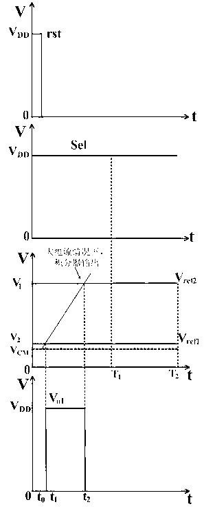
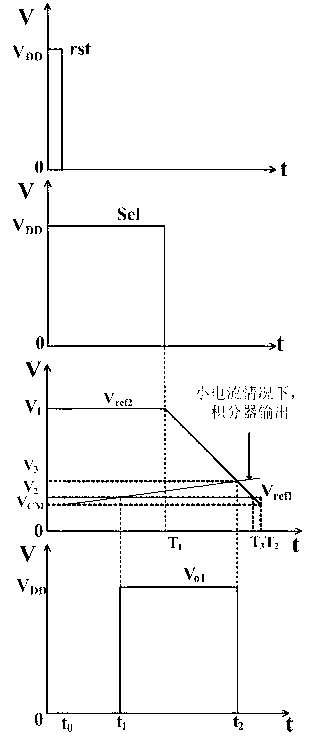
[0025] The structure of the circuit is as figure 1 As shown, the circuit is divided into two circuits, one for photocurrent detection, and one for photodiode leakage current and dark current detection. Each way includes photodiode, integrator, comparator and logic gate circuit. The reference voltage source of the circuit composed of a fixed reference voltage and a ramp signal generator. For this path of photocurrent detection, the photodiode D1 converts the light signal into a current signal. Switch S 1 , the feedback capacitor C f1 It forms an integrator with the operational amplifier OP1, and converts the current signal into a voltage signal. The output of the integrator is connected to the inverting inputs of two identical comparators CMP1 and CMP2. The positive input terminal of CMP1 is connected to the fixed reference voltage V 1 , the positive input of CMP2...


PUM


Abstract

The invention belongs to the technical field of fluorescent detection, and particularly relates to a pulse width modulation-based fluorescent detection and optical-to-digital conversion system. The pulse width modulation-based fluorescent detection and optical-to-digital conversion system comprises an optical current detection circuit, a dark current detection circuit, a reference voltage source, a wireless transmitting module and a wireless receiving end, wherein the wireless receiving end consists of a wireless receiver and an MCU (Micro Controller Unit). Detection of output current of a photodiode is divided into a resetting phase, a heavy current detection phase and a low current detection phase. At the resetting phase, an integrator and a ramp signal generator are reset to initial states. At the heavy current detection phase, reference voltage of a comparator is kept at a fixed level by a reference voltage control signal Sel. At the low current detection phase, the reference voltage of the comparator is controlled to be a ramp signal by the Sel signal. By using the pulse width modulation-based fluorescent detection and optical-to-digital conversion system, conversion from a fluorescent signal to a digital signal at low power consumption and transmission and reception of fluorescent detection data can be realized, and the detection accuracy and the dynamic range of the fluorescent signal by the circuit are improved.

Description

technical field [0001] The invention belongs to the technical field of fluorescence detection, and in particular relates to a circuit for converting an output voltage of an integrator into a pulse width modulation signal in a fluorescence detection circuit. Background technique [0002] Fluorescence detection is to generate fluorescence through the chemical reaction between luciferase and the detected compound, and determine the concentration of the detected substance by detecting the intensity of the fluorescence and expressing it in digital form. Because of its fast detection speed and high sensitivity, it has been widely used. [0003] The fluorescent detection circuit converts the fluorescent signal into a photocurrent signal through a photodiode, and converts the current signal into a voltage signal through an integrator. Traditional fluorescence detection circuits quantify voltage signals through high-resolution ADCs. This brings two disadvantages: 1. The accuracy of...

Claims


Application Information

Patent Timeline
Patent Type & Authority Applications(China)
IPC IPC(8): G01N21/64
Inventor 秦亚杰万磊
Owner FUDAN UNIV
Why Eureka
Try Eureka