

Method for manufacturing soft silicon-based thin film solar cell integrated component
A silicon-based thin film and solar cell technology, applied in electrical components, circuits, semiconductor devices, etc., can solve the problems of expensive wires and equipment, and achieve the effects of reducing difficulty, improving reliability, and protecting areas
- Summary
- Abstract
- Description
- Claims
- Application Information
AI Technical Summary
Problems solved by technology
Method used
Image

Examples
Embodiment Construction
[0022] The present invention will be further elaborated below in conjunction with the accompanying drawings and specific embodiments. These examples should be understood as only for illustrating the present invention but not for limiting the protection scope of the present invention. After reading the contents of the present invention, those skilled in the art can make various changes or modifications to the present invention, and these equivalent changes and modifications also fall within the scope defined by the claims of the present invention.
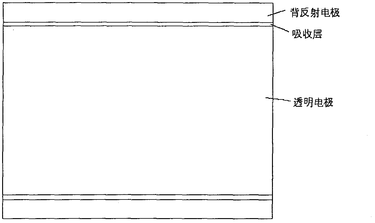
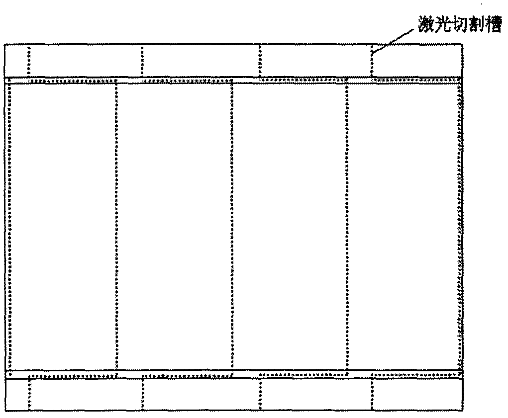
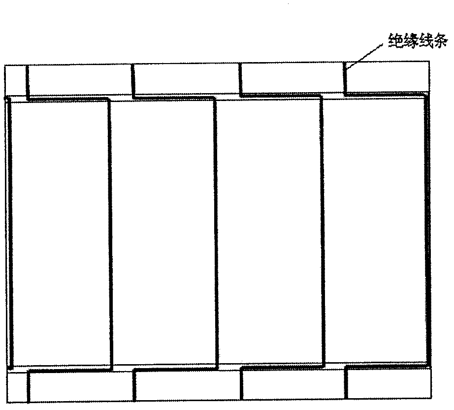
[0023] 1. A roll of flexible polyimide (thickness 125um) is sequentially passed through the vacuum chamber, and the Ag / ZnO back reflection layer is grown by magnetron sputtering, the Ag thickness is 300nm, and the ZnO thickness is 500nm; the amorphous silicon nip structure, the n layer is 30nm, i layer 300nm, p layer 15nm, ITO transparent conductive film, ITO thickness 80nm. The vacuum chamber adopts cover plate, baffle or other te...
PUM
 Abstract
Description
Claims
Application Information