MEMS (micro-electromechanical systems) device and vacuum encapsulation method of wafer level thereof

A device and silicon structure technology, which is applied in the field of MEMS devices and their vacuum packaging based on silicon-silicon bonding technology, can solve the problems of poor air tightness and difficult electrical interconnection of MEMS devices in wafer-level vacuum packaging, and is convenient for promotion and application. , Reduce the cost of packaging, good air tightness

Active Publication Date: 2013-01-09
EAST CHINA INST OF OPTOELECTRONICS INTEGRATEDDEVICE
View PDF8 Cites 20 Cited by
  • Summary
  • Abstract
  • Description
  • Claims
  • Application Information

AI Technical Summary

Problems solved by technology

[0005] The purpose of the present invention is to solve the problems of poor airtightness and difficulty in electrical interconnection of MEMS device waf

Method used


Image

  • MEMS (micro-electromechanical systems) device and vacuum encapsulation method of wafer level thereof
  • MEMS (micro-electromechanical systems) device and vacuum encapsulation method of wafer level thereof
  • MEMS (micro-electromechanical systems) device and vacuum encapsulation method of wafer level thereof

Examples


Example Embodiment

[0021] The present invention will be further described below in conjunction with the drawings.

[0022] 1. MEMS device structure:

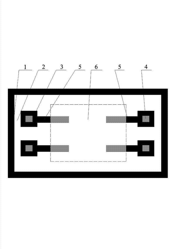
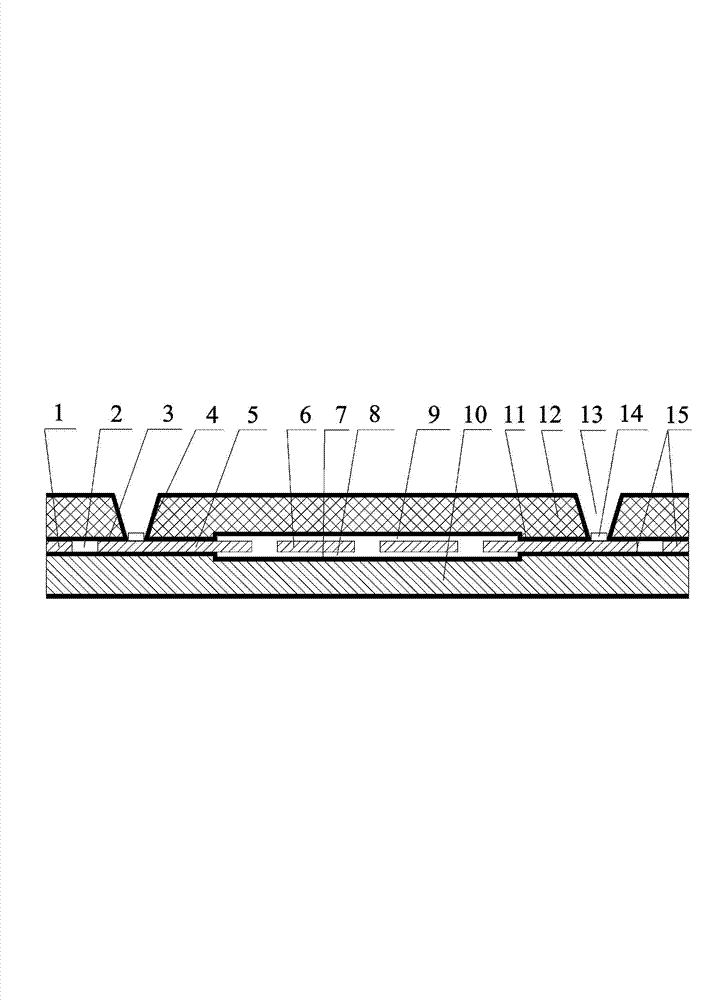
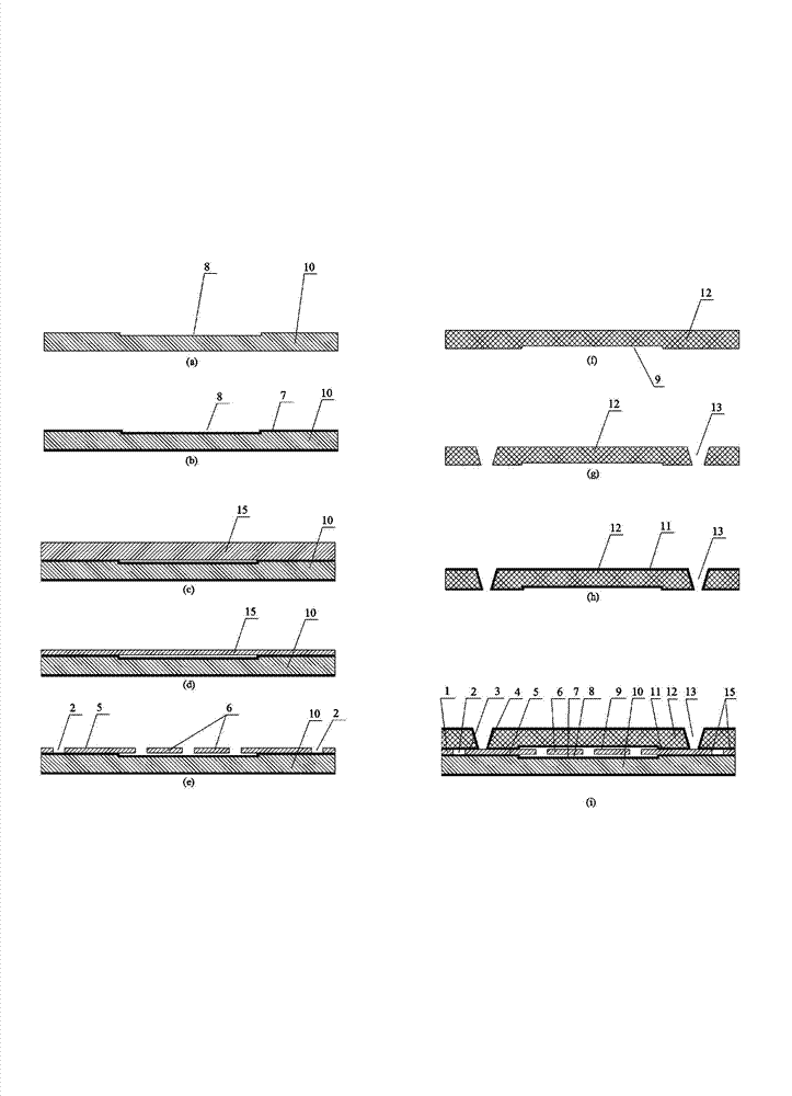
[0023] Such as figure 1 , figure 2 As shown, the MEMS device is composed of a silicon substrate layer 10, a silicon structure layer 15 and a silicon cap layer 12.

[0024] The surface of the silicon substrate 10 is etched to form a shallow cavity 8 so that a certain distance is formed between the movable structure 6 and the substrate to avoid hindering the movement of the movable structure. The silicon cap layer 12 etches the shallow cavity 9 and the lead through hole 13, and the shallow cavity 9 corresponds to the position and shape of the shallow cavity 8 on the silicon substrate. The surface of the silicon substrate 10 and the silicon cap 12 respectively have a certain thickness of an oxide layer 7 and an oxide layer 11, which are bonded to the silicon structure layer 15 to serve as insulation. The silicon structure layer 15 is composed of a movabl...


PUM


Abstract

The invention relates to an MEMS (micro-electromechanical systems) device and a vacuum encapsulation method of the wafer level thereof. The device is characterized in that wafer level vacuum encapsulation is realized by adopting a silicon-silicon direct bonding technology, a low-resistance silicon wafer is adopted in a silicon structure layer (15) bonded to a silicon substrate, and is directly etched on the silicon layer to form an electrical interconnection lead wire (5); and aluminum electrode (14) is sputtered on an electrical interconnection lead wire bonding area (4) in a lead wire through hole (13) of a silicon nut cap (12). The device has the advantages that a total silicon structure is adopted, and no residual stress exits after bonding, so that the working performance of the device can be greatly improved; low-resistance silicon is utilized as an electrode lead wire, so that damage of high temperature to a metal electrode in the silicon-silicon direct bonding process can be avoided; and the silicon-silicon direct bonding air tightness is extremely good, so that the encapsulation cost is greatly reduced. The method is high in accordance and reliability, and the process is easily implemented.

Description

technical field [0001] The invention belongs to the field of micro-electromechanical technology, in particular to a MEMS device based on silicon-silicon bonding technology and a vacuum packaging method thereof. Background technique [0002] Micro Electro-Mechanical Systems (MEMS) is based on microelectronics, micromechanics and material science to research, design and manufacture micro devices with specific functions, including micro sensors, micro actuators, etc. MEMS devices have volume Small size, light weight, low power consumption, mass production and many other advantages. [0003] Usually MEMS devices are composed of some movable structures, which are very fragile, fragile, and easily damaged by dust, water vapor, etc. In order not to affect subsequent processing and assembly, they need to be packaged at wafer level to provide good Mechanical support and environmental protection and other functions. In addition, many MEMS devices with important applications require ...

Claims


Application Information

Patent Timeline
IPC IPC(8): B81B7/00B81C3/00
Inventor 何凯旋郭群英陈博王鹏汪祖民王文婧黄斌陈璞徐栋吕东锋
Owner EAST CHINA INST OF OPTOELECTRONICS INTEGRATEDDEVICE
Why Eureka
Try Eureka