Off-axis signal processing method

A signal processing, off-axis technology, applied in optics, instruments, photolithography process of pattern surface, etc., can solve the problems of large amount of calculation, reduced productivity, and more time-consuming, so as to reduce alignment accuracy and improve productivity. rate, the effect of reducing computation time

Active Publication Date: 2013-01-09
SHANGHAI MICRO ELECTRONICS EQUIP (GRP) CO LTD
View PDF8 Cites 1 Cited by
  • Summary
  • Abstract
  • Description
  • Claims
  • Application Information

AI Technical Summary

Problems solved by technology

[0011] The calculation of the fitting calculation is very heavy, especially when there are many sampling points, the fitting calculation will take more time, resulting in a decrease in yield

Method used


Image

  • Off-axis signal processing method
  • Off-axis signal processing method
  • Off-axis signal processing method

Examples


Embodiment Construction

[0022] The idea, specific structure and technical effects of the present invention will be further described below in conjunction with the accompanying drawings, so as to fully understand the purpose, features and effects of the present invention.

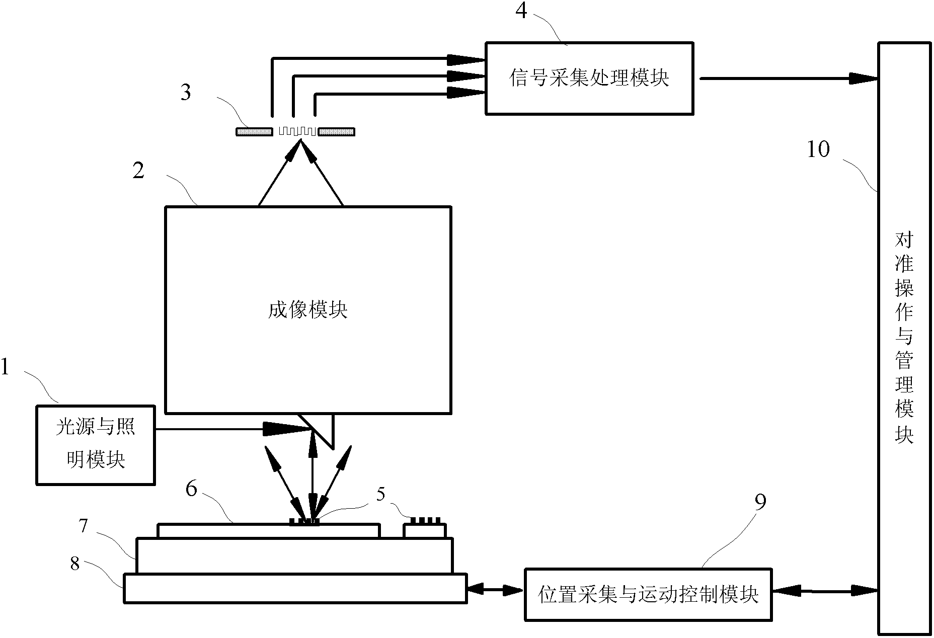
[0023] figure 1 is a schematic diagram of an off-axis alignment system according to a preferred embodiment of the present invention. Please refer to figure 1 . In this embodiment, the off-axis alignment system includes a light source and lighting module 1, an imaging module 2, a reference grating 3, a signal acquisition and processing module 4, an alignment mark 5, a workpiece table 7, a motion table 8, position acquisition and motion control module 9 and alignment operation and management module 10 . The workpiece table 7 carries the silicon wafer 6 .

[0024] In this embodiment, the light source and the illumination module 1 provide illumination light beams to irradiate the alignment marks 5 to form diffracted light carrying ...


PUM


Abstract

The invention discloses an off-axis signal processing method, comprising the following steps: (a) determining a linear fitting model containing direct-current level, sine coefficient and cosine coefficient; (b) conducting off-axis aligning scanning to acquire position sampling signals and light intensity sampling signals; (c) extracting characteristic frequency signals from the light intensity sampling signals and conducting Fourier transform, and calculating values of the sine coefficient and cosine coefficient; and (d) calculating the position sampling signals and light intensity sampling signals according to the values of the sine coefficient and cosine coefficient. According to the invention, the aligning accuracy can not be reduced, and simultaneously the calculation time is greatly reduced, thus the yield is raised.

Description

technical field [0001] The invention relates to the field of photolithographic production of semiconductor integrated circuits, in particular to an off-axis signal processing method. Background technique [0002] In the process of using a lithography machine for the production of integrated circuit chips, in order to achieve the desired overlay accuracy of the lithography machine, it is necessary to accurately establish the relationship between the coordinate systems of the lithography machine. Off-axis alignment is irradiated on the silicon wafer mark The reflected light of the polarized laser is then diffracted to form the alignment between the diffraction mark and the reference mark of the silicon wafer. Since the silicon wafer mark is attached to the silicon wafer or the silicon wafer stage, the alignment can be formed by moving the worktable at a constant speed Alignment scan between markers and reference markers. [0003] US Patent US6297876B1 and Chinese Patents CN03...

Claims


Application Information

Patent Timeline
Patent Type & Authority Applications(China)
IPC IPC(8): G03F9/00G03F7/20
Inventor 朱正平李运锋宋海军李欣欣
Owner SHANGHAI MICRO ELECTRONICS EQUIP (GRP) CO LTD
Why Eureka
Try Eureka