Optical fiber and optical waveguide coupling method and structure and wafer testing method

An optical waveguide coupling and optical fiber technology, applied in the field of optical chips, can solve problems such as increasing the size of the device, and achieve the effects of improving the coupling efficiency and reducing the alignment accuracy and tolerance.

Inactive Publication Date: 2021-10-29
CENT SOUTH UNIV
View PDF5 Cites 0 Cited by
  • Summary
  • Abstract
  • Description
  • Claims
  • Application Information

AI Technical Summary

Problems solved by technology

From the point of view of alignment, the optical fiber of the grating coupling method must not only maintain a certain distance from the grating in the horizontal direction, but also ensure a certain height in the vertical direction. This requires the design of a special fixture to ensure the accuracy of the vertical coupling. greatly increases the size of the device

Method used


Image

  • Optical fiber and optical waveguide coupling method and structure and wafer testing method
  • Optical fiber and optical waveguide coupling method and structure and wafer testing method
  • Optical fiber and optical waveguide coupling method and structure and wafer testing method

Examples


Embodiment Construction

[0027] It should be noted that, in the case of no conflict, the embodiments in the present application and the features in the embodiments can be combined with each other. The present application will be described in detail below with reference to the accompanying drawings and embodiments.

[0028] It should be noted that the steps shown in the flowcharts of the accompanying drawings may be performed in a computer system, such as a set of computer-executable instructions, and that although a logical order is shown in the flowcharts, in some cases, The steps shown or described may be performed in an order different than here.

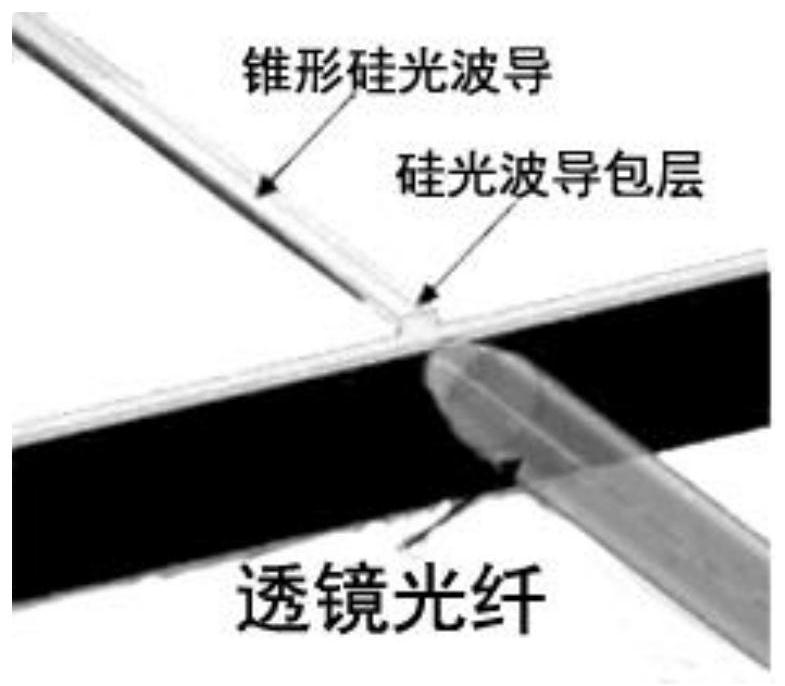
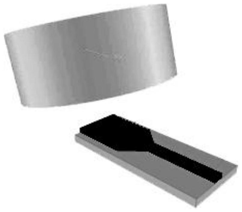
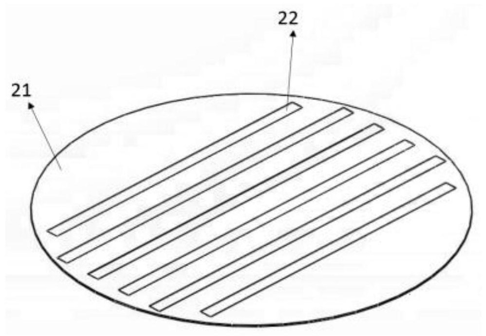
[0029] In this embodiment, the wafer-level packaging technology takes the wafer as the processing object, performs coupling packaging and testing on many chips on the wafer, and then cuts the wafer into single chips. High-throughput functional testing of silicon photonics is a key issue in large-scale chip manufacturing, and the most effective coupling ...


PUM


Abstract

The invention discloses an optical fiber and optical waveguide coupling method and structure and a wafer testing method. The coupling method comprises the following steps: manufacturing a required waveguide in a block of a wafer; etching a groove in one end of the waveguide, wherein the groove is used for inserting an optical fiber in the direction in which the waveguide forms a first preset angle; cutting the end surface of the optical fiber to be inserted into the groove into a second preset angle, and coating a layer of anti-reflection film on the cut surface; and inserting the cut optical fiber into the groove, wherein light passing through the optical fiber enters the waveguide after being emitted by the anti-reflection film. According to the invention, the problem of the coupling mode between the single-mode optical fiber and the silicon optical waveguide in the optical chip test in the prior art is solved, so that the coupling efficiency of the optical fiber and the silicon optical waveguide is improved, and the alignment precision and tolerance are reduced.

Description

technical field [0001] The present application relates to the field of optical chips, in particular, to a method and structure for coupling an optical fiber and an optical waveguide, and a wafer testing method. Background technique [0002] Photonic integrated circuits were first proposed by Dr. Miller of Bell Laboratories in the United States in 1969. Active devices such as lasers, modulators, and detectors were integrated on the same substrate through advanced lithography technology, and optical waveguides, isolators, Passive components such as couplers and filters are connected to form a micro-optical system, which realizes the integration and miniaturization of the optical information processing system and reduces the manufacturing cost of the chip. With the development of optical communication today, there are many kinds of optoelectronic integrated devices, and its integration requires the integration of discrete optical components with different functions on the same ...

Claims


Application Information

Patent Timeline
Patent Type & Authority Applications(China)
IPC IPC(8): G02B6/24G02B6/25G02B6/36H01L21/66
CPCG02B6/24G02B6/25G02B6/364H01L22/12
Inventor 郑煜郜飘飘段吉安
Owner CENT SOUTH UNIV
Why Eureka
Try Eureka