Radio frequency power transistor based on inversion process and forming method thereof

A technology of radio frequency power and process, which is applied in the field of radio frequency power tube and its formation based on inversion process, can solve the problems such as difficulty in guaranteeing process accuracy, difficulty in gate control ability, difficulty in gate oxide layer, etc., to achieve high device structure accuracy, Effects of improving device performance and reducing device area

Active Publication Date: 2013-01-09
TSINGHUA UNIV
View PDF4 Cites 1 Cited by
  • Summary
  • Abstract
  • Description
  • Claims
  • Application Information

AI Technical Summary

Problems solved by technology

Its disadvantage is that it is difficult to form the gate oxide layer of High-K dielectric material on the graphene film, and it is often difficult to achieve a smaller equivalent oxide thickness (equivalent oxide thinness, EOT) because of the introduction of ion modification, so it is difficult to improve the gate oxide layer. controllability; in the process of simultaneously forming the gate, source and drain on the graphene film, the process accuracy is difficult to be guaranteed; and the resistance of the source-drain contact of the final device is relatively large
Carrying too many process steps on the graphene film is not good for protecting its excellent electrical properties, such as the deterioration of the performance of graphene by photoresist during multiple photolithography processes, and the deterioration of the performance of High-K materials by possible wet etching, etc. Wait

Method used


Image

  • Radio frequency power transistor based on inversion process and forming method thereof
  • Radio frequency power transistor based on inversion process and forming method thereof
  • Radio frequency power transistor based on inversion process and forming method thereof

Examples


Embodiment Construction

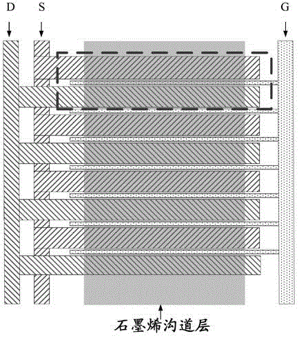
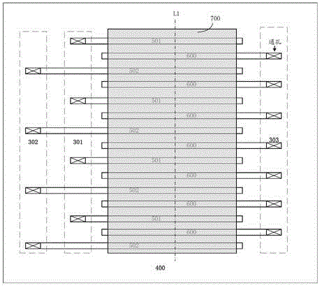
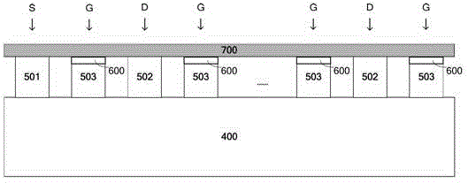
[0030] Embodiments of the present invention are described in detail below, examples of which are shown in the drawings, wherein the same or similar reference numerals designate the same or similar elements or elements having the same or similar functions throughout. The embodiments described below by referring to the figures are exemplary only for explaining the present invention and should not be construed as limiting the present invention.

[0031] In describing the present invention, it should be understood that the terms "longitudinal", "transverse", "upper", "lower", "front", "rear", "left", "right", "vertical", The orientation or positional relationship indicated by "horizontal", "top", "bottom", "inner", "outer", etc. are based on the orientation or positional relationship shown in the drawings, and are only for the convenience of describing the present invention and simplifying the description, rather than Nothing indicating or implying that a referenced device or elem...


PUM


Abstract

The invention discloses a radio frequency power transistor based on an inversion process and a forming method thereof. The method comprises the following steps of: providing a substrate; forming a transition layer; forming a source connecting wire, a drain connecting wire and a gate connecting wire; forming interlayer dielectric layers on the transition layer, and filling the interlayer dielectric layers between the connecting wires; forming metal contact layers on the interlayer dielectric layers, and connecting the metal contact layers with the connecting wires; etching the metal contact layers to form N sources, N drains and 2N-1 gates, which are parallel mutually, wherein the sources, the gates and the drains are adjacently arranged sequentially according to the order of source-gate-drain-gate, the N sources are connected with the source connecting wire, the N drains are connected with the drain connecting wire, and the 2N-1 gates are connected with the gate connecting wire; forming a gate dielectric layer; and forming a graphene thin film as a channel layer. According to the method disclosed by the invention, the inversion process is adopted, the implementation is easy, and the method is stable and reliable; and the device disclosed by the invention has an inversion structure, the source-drain contact is small, and the gate control ability is strong.

Description

technical field [0001] The invention relates to the technical field of semiconductors, in particular to a radio frequency power tube based on an inversion process and a forming method thereof. Background technique [0002] The device serving as the final output in the amplifying circuit is called an RF power tube based on an inversion process. Most of the existing RF power tubes are composed of multiple silicon-based FETs connected in parallel, but due to the limitation of the mobility of the channel layer material, there is limited room for improving the performance of the RF power tube. Therefore, research and development of RF power tubes with new materials and new structures has become a research hotspot. [0003] In recent years, studies have shown that graphene materials have excellent performance characteristics such as high intrinsic carrier mobility, high strong field drift velocity, high current carrying capacity (an order of magnitude higher than that of metals),...

Claims


Application Information

Patent Timeline
Patent Type & Authority Applications(China)
IPC IPC(8): H01L21/336H01L29/78H01L21/28H01L29/45
Inventor 吕宏鸣肖柯吴华强钱鹤伍晓明
Owner TSINGHUA UNIV
Why Eureka
Try Eureka