Light emitting diode (LED) with inverted structure and manufacturing method thereof

A light-emitting diode, flip-chip technology, applied in electrical components, circuits, semiconductor devices, etc., can solve the problems of thermal conductivity, reduced electrical conductivity, poor controllability, difficult processing, etc., to improve thermal conductivity and electrical conductivity, temperature and time. Ease of control, improved bond strength

Active Publication Date: 2013-01-23
LEDMAN OPTOELECTRONIC HZ CO LTD
View PDF10 Cites 10 Cited by
  • Summary
  • Abstract
  • Description
  • Claims
  • Application Information

AI Technical Summary

Problems solved by technology

[0009] 1. Flip-chip soldering usually uses Au-Sn (gold-tin) solder, which has defects such as high melting point, high price, brittle performance, and difficult processing.
Since the eutectic temperature of gold-tin alloy is around 300°C, and the melting point of the alloy is very sensitive to the composition near the eutectic temperature, the requirements for the thickness and composition of the electrode and substrate coating are very strict; the thermal conductivity of Au-Sn alloy is commonly used Solder is relatively high, and its thermal conductivity range is usually only 50-60W / mK; overall, the process has high requirements on machine performance, process parameters, environmental conditions and personnel skills, and the controllability is poor
[0010] 2. When using lead-free solder paste and silver glue for flip-chip bonding, since both the solder paste and silver glue contain certain organic polymer components, the alloy formed by the solder paste after reflow soldering will have organic residues, and There are many microscopic cavities, which will reduce its thermal conductivity and electrical conductivity; the thermal conductivity of the commonly used silver glue is also low, and the cured colloid is blocked by organic polymers, and the silver particles in the colloid cannot form well. It is difficult to meet the performance requirements of thermal and conductive materials in the flip chip process

Method used


Image

  • Light emitting diode (LED) with inverted structure and manufacturing method thereof
  • Light emitting diode (LED) with inverted structure and manufacturing method thereof
  • Light emitting diode (LED) with inverted structure and manufacturing method thereof

Examples


Embodiment Construction

[0034] The present invention will be described in detail below in conjunction with the accompanying drawings and embodiments.

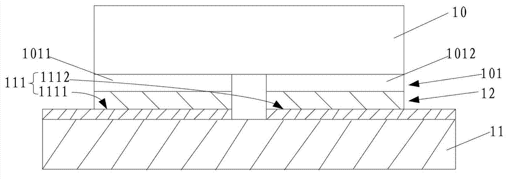
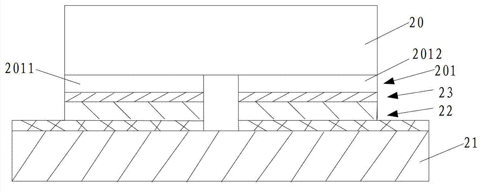
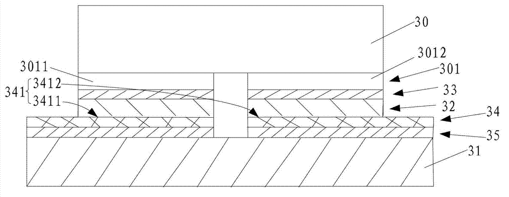
[0035] refer to figure 1 , figure 1 It is a structural schematic diagram of the first embodiment of the light-emitting diode with the flip-chip structure of the present invention. The light emitting diode according to the embodiment of the present invention includes: a wafer 10 , a substrate 11 and a nano-silver layer 12 .

[0036] The electrode layer 101 is formed on at least one surface of the wafer 10 , and at least the surface of the substrate 11 adjacent to the wafer 10 is a metal surface 111 . The electrode layer 101 includes a wafer positive electrode 1011 and a wafer negative electrode 1012 that are insulated from each other. Usually, the electrode layer 101 is formed by plating a metal film on the P electrode (not shown) and the N electrode (not shown) of the wafer 10. Further, the P The electrode is coated with a metal film as the positiv...


PUM


Abstract

The invention discloses a light emitting diode (LED) with an inverted structure. The LED comprises a chip and a substrate, wherein an electrode layer is formed on at least one surface of the chip; at least one surface, which is close to one side of the chip, of the substrate is a metal surface; the electrode layer comprises a chip anode and a chip cathode which are insulated from each other; the metal surface of the substrate comprises an anode metal region and a cathode metal region, correspond to the chip anode and the chip cathode, which are insulated from each other; and nano silver layers are respectively arranged between the chip anode and the anode metal region and between the chip cathode and the cathode metal region. The invention also discloses a method for manufacturing the LED with the inverted structure. Due to the mode, the thermal conductivity and electric conductivity can be improved, and the bonding strength between the chip and the substrate can be improved.

Description

technical field [0001] The invention relates to the technical field of light-emitting diode packaging, in particular to a light-emitting diode with a flip-chip structure and a preparation method thereof. Background technique [0002] LED (Light Emitting Diode, Light Emitting Diode), as the fourth generation of green lighting source, has been widely used at present. With the improvement of LED chip integration and the demand for power LEDs, the heat dissipation of high-power LEDs has become an urgent problem to be solved. Because the junction temperature of the LED chip is relatively sensitive to temperature, if the heat cannot be dissipated in time, it will not only accelerate the light decay, but also reduce its service life. [0003] The positive mounting structure of the traditional LED chip is used. On the one hand, the light-emitting area will be reduced due to the existence of the metal electrode, and the metal electrode has a certain light-absorbing effect, thereby re...

Claims


Application Information

Patent Timeline
Patent Type & Authority Applications(China)
IPC IPC(8): H01L33/48H01L33/62
Inventor 李漫铁屠孟龙李扬林
Owner LEDMAN OPTOELECTRONIC HZ CO LTD
Why Eureka
Try Eureka