Low-cost TSV (through silicon via) three-dimensional integration process method

A process method and low-cost technology, applied in the field of microelectronics, can solve the problems of expensive investment in special equipment, difficult to remove the bottom insulating film, and difficult to protect the side wall of the hole, so as to save investment in special equipment, save special equipment, reduce cost effect

Inactive Publication Date: 2013-01-30
NO 771 INST OF NO 9 RES INST CHINA AEROSPACE SCI & TECH
View PDF4 Cites 12 Cited by
  • Summary
  • Abstract
  • Description
  • Claims
  • Application Information

AI Technical Summary

Problems solved by technology

The characteristic of this method is to keep the insulating film between the barrier layer and the seed layer and the side wall of the through hole, and remove the insulating film at the bottom. It is difficult for glue equipment to form a good protection for the sidewall of the through hole, and when etching the bottom insulating layer of the TSV through hole, it is difficult to completely and cleanly remove the bottom insulating film, and the subsequent deglue process is also a big challenge
At present, the common targeted method is to use TSV special glue spraying equipment, large depth of field exposure machine, special etching and glue removal equipment. The disadvantage of this process is that the special equipment is expensive, the process is cumbersome, and the efficiency is low.

Method used


Image

  • Low-cost TSV (through silicon via) three-dimensional integration process method
  • Low-cost TSV (through silicon via) three-dimensional integration process method
  • Low-cost TSV (through silicon via) three-dimensional integration process method

Examples


Embodiment 1

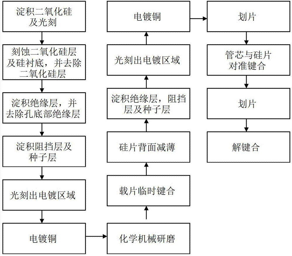
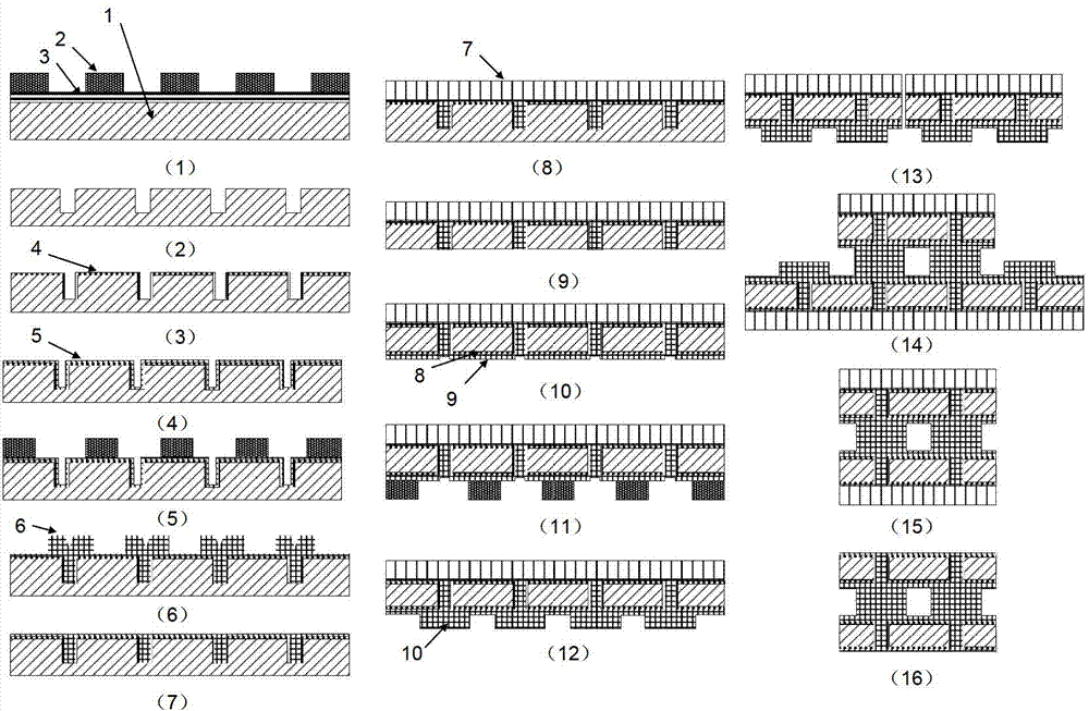
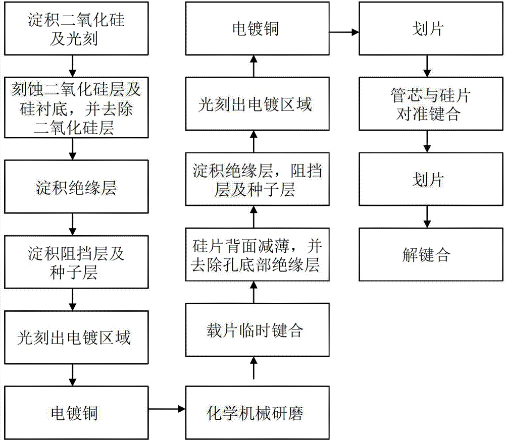
[0037] 1. Use Cz silicon (100) (0.1~0.2Ω·cm) substrate; use LPCVD to deposit silicon dioxide 1500A, coat photoresist 10000A on the surface of the silicon wafer, expose and develop, and expose the silicon dioxide with a width of 200000A silicon surface

[0038] 2. Etch silicon dioxide to the surface of the silicon substrate, and continue to etch the silicon substrate to form a TSV hole with a depth of 500000A;

[0039]3. SPM cleaning to remove the photoresist on the surface, and LPCVD to deposit a silicon dioxide insulating film 150A;

[0040] 4. Using ion sputtering to grow the barrier layer tantalum nitride 150A, and the seed layer copper 150A;

[0041] 5. Apply photoresist 10000A on the surface of the silicon wafer again, expose, develop, and expose the window that needs copper plating;

[0042] 6. Electroplate copper 600000A on the surface of the silicon wafer, and use SPM to clean and remove the photoresist;

[0043] 7. Using chemical mechanical grinding, grinding to th...

Embodiment 2

[0054] 1. Use Cz silicon (100) (0.1~0.2Ω·cm) substrate; use LPCVD to deposit silicon dioxide 1500A, coat photoresist 10000A on the surface of the silicon wafer, expose and develop, and expose the silicon dioxide with a width of 250000A silicon surface

[0055] 2. Etch silicon dioxide to the surface of the silicon substrate, and continue to etch the silicon substrate to form a TSV hole with a depth of 550000A;

[0056] 3. SPM cleaning to remove the photoresist on the surface, and LPCVD to deposit a silicon dioxide insulating film 150A;

[0057] 4. Using ion sputtering to grow the barrier layer tantalum nitride 150A, and the seed layer copper 150A;

[0058] 5. Apply photoresist 10000A on the surface of the silicon wafer again, expose, develop, and expose the window that needs copper plating;

[0059] 6. Electroplate copper 650000A on the surface of the silicon wafer, and use SPM to clean and remove the photoresist;

[0060] 7. Using chemical mechanical grinding, grinding to t...

Embodiment 3

[0071] 1. Use Cz silicon (100) (0.1~0.2Ω·cm) substrate; use LPCVD to deposit silicon dioxide 1500A, coat photoresist 10000A on the surface of the silicon wafer, expose and develop, and expose the silicon dioxide with a width of 300000A silicon surface

[0072] 2. Etch silicon dioxide to the surface of the silicon substrate, and continue to etch the silicon substrate to form a TSV hole with a depth of 600000A;

[0073] 3. SPM cleaning to remove the photoresist on the surface, and LPCVD to deposit a silicon dioxide insulating film 150A;

[0074] 4. Using ion sputtering to grow the barrier layer tantalum nitride 150A, and the seed layer copper 150A;

[0075] 5. Apply photoresist 10000A on the surface of the silicon wafer again, expose, develop, and expose the window that needs copper plating;

[0076] 6. Electroplate copper 700000A on the surface of the silicon wafer, and use SPM to clean and remove the photoresist;

[0077] 7. Using chemical mechanical grinding, grinding to t...


PUM


Abstract

The invention discloses a low-cost TSV (through silicon via) three-dimensional integration process method. The method is characterized in that barrier layer and seeding layer fabrication steps, and a copper plating step are directly carried out after an insulation layer is fabricated on the side wall of a TSV. In comparison with the conventional TSV process, the method obviates six steps of gluing, exposure, development, CD (critical dimension) measurement, silicon dioxide etching, and resist removal; and an over-thinning step is carried out moderately to remove the insulation layer on the bottom of the TSV while thinning the back side of a wafer, so that all processes are substantially in the same plane to obviate photolithography and etching steps which are carried out in the prior art to remove the insulation layer on the bottom of the TSV with a depth of tens of micrometers, thereby obviating the need for expensive special equipment. The low-cost TSV three-dimensional integration process method provided by the invention has the advantages of short process flow, high efficiency, and low process cost.

Description

technical field [0001] The invention relates to the technical field of microelectronics. Background technique [0002] The traditional TSV three-dimensional integration is to form a photoresist protection on the side wall of the through hole after the side wall insulation process of the through hole is completed, etch away the bottom insulating layer, and then make a barrier layer and a seed layer and electroplate copper. For example, the papers published by IMEC and the patents that have been applied for (200910082236.3 "A Manufacturing Method for the Insulating Layer of TSV Via Holes") and so on. The characteristic of this method is to keep the insulating film between the barrier layer and the seed layer and the side wall of the through hole, and remove the insulating film at the bottom. It is difficult for glue equipment to form a good protection for the sidewall of the through hole, and when etching the bottom insulating layer of the TSV through hole, it is difficult to...

Claims


Application Information

Patent Timeline
Patent Type & Authority Applications(China)
IPC IPC(8): H01L21/768
Inventor 单光宝李翔孙有民蔚婷婷付鹏
Owner NO 771 INST OF NO 9 RES INST CHINA AEROSPACE SCI & TECH
Why Eureka
Try Eureka