All Al-BSF crystal silicon cell and preparation method thereof

A technology of crystalline silicon battery and all-aluminum back field, which is applied in the direction of circuits, electrical components, semiconductor devices, etc., can solve the problems of unfavorable product market competitiveness, increase the preparation process, increase production cost, etc., and achieve improved field passivation characteristics, Effect of improving spectral response and improving conversion efficiency

Inactive Publication Date: 2013-01-30
HUNAN RED SUN PHOTOELECTRICITY SCI & TECH
View PDF3 Cites 12 Cited by
  • Summary
  • Abstract
  • Description
  • Claims
  • Application Information

AI Technical Summary

Problems solved by technology

Whether it is to increase the preparation process or adopt high-end equipment, it will increase t

Method used


Image

  • All Al-BSF crystal silicon cell and preparation method thereof
  • All Al-BSF crystal silicon cell and preparation method thereof
  • All Al-BSF crystal silicon cell and preparation method thereof

Examples


Embodiment 1

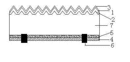
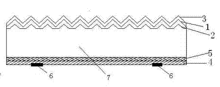
[0047] A kind of all-aluminum back field crystalline silicon cell, such as figure 2 As shown, a silicon layer 7 is included, and a P+ passivation layer 5 and an aluminum back conductive layer 4 are laminated on the back of the silicon layer 7 in sequence, and a back electrode 6 is provided on the aluminum back conductive layer 4 .

[0048] The back electrode 6 is a tin electrode. The thickness of the aluminum back conductive layer is 10 microns-30 microns.

Embodiment 2

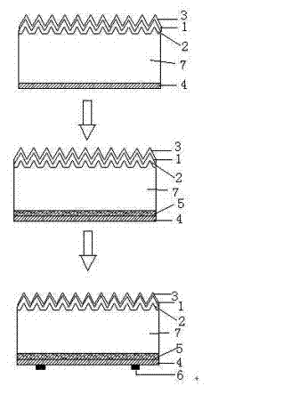
[0050] A method for preparing an all-aluminum back field crystalline silicon cell, the preparation process is as follows image 3 As shown, the steps are:

[0051] a) Attach aluminum paste on the back of the silicon nitride anti-reflective coating and dry it to form an aluminum back conductive layer with a thickness of 25 microns, and the drying temperature is 240 ° C;

[0052] b) Print a silver grid line on the surface of the silicon wafer to form a positive electrode and dry it at 200°C;

[0053] c) High temperature sintering, the sintering temperature is 850°C, to form a P+ passivation layer;

[0054] d) Attach tin paste on the conductive layer on the aluminum back as the back electrode and dry it at a temperature of 170°C;

[0055] e) Low temperature sintering, the sintering temperature is 300°C, so that the adhesion between the back electrode and the aluminum back conductive layer is 3N, and the preparation of the all-aluminum back field crystalline silicon cell is comp...

Embodiment 3

[0058] A method for preparing an all-aluminum back field crystalline silicon cell, the preparation process is as follows Figure 4 As shown, the steps are:

[0059]a) Attach aluminum paste on the back of the silicon nitride anti-reflection film layer and dry it to form an aluminum back conductive layer. The drying temperature is 250 ° C;

[0060] b) Print a silver grid line on the surface of the silicon wafer layer as a positive electrode and dry it at 200°C;

[0061] c) High temperature sintering, the sintering temperature is 900°C, to form a P+ passivation layer;

[0062] d) Use laser ablation, mechanical method or corrosion method to remove the surface layer on the aluminum back conductive layer at the position where the back electrode is attached to form a window for removing the surface layer, and the thickness of the removal layer is 0.1 μm-3 μm;

[0063] e) Screen-print silver paste on the conductive layer on the aluminum back as the back electrode and dry it. The sta...


PUM

PropertyMeasurementUnit
Thicknessaaaaaaaaaa
Viscosityaaaaaaaaaa
Viscosityaaaaaaaaaa

Abstract

The invention discloses an all Al-BSF crystal silicon cell and a preparation method thereof. The all Al-BSF crystal silicon cell comprises a silicon wafer layer (7), wherein a P+ passivation layer (5) and an Al-BSF conducting layer (4) are sequentially bonded on a back face of the silicon wafer layer (7); and a back electrode (6) is arranged on the Al-BSF conducting layer (4). The method comprises the following steps of: printing one layer of aluminium paste on all positions of a back face of a solar cell expect for edges; printing the back electrode; and forming the P+ passivation layer on an electrode area through sintering. Due to the structure of the cell, direct contact of silver and a silicon wafer is avoided, so that the complex defects of a back electrode area is greatly reduced; the photoelectric conversion efficiency of the crystal silicon cell can be greatly improved; and compared with a preparation manner of a general cell, an overlapping area of the back electrode and BSF can be neglected, and the width of the electrode can be reduced, so that the production cost is reduced.

Description

technical field [0001] The invention relates to the field of back field preparation of crystalline silicon batteries, in particular to a crystalline silicon battery and a preparation method thereof. Background technique [0002] A solar cell is a semiconductor device that can convert solar energy into electrical energy. Under the condition of light, a photogenerated current will be generated inside the solar cell, and the electrical energy can be output through the electrodes. A solar cell structure with P-type silicon typically has its negative electrode on the front side of the cell and its positive electrode on the back. When illuminated with light, radiation of the appropriate wavelength results in the creation of hole-electron pairs in the semiconductor. The potential difference that exists across the P-N junction causes holes and electrons to migrate across the junction in opposite directions, creating a flow of current that transfers electrical energy to an external ...

Claims


Application Information

Patent Timeline
IPC IPC(8): H01L31/0224H01L31/18
CPCY02P70/50
Inventor 郭进姬常晓刘文峰任哲
Owner HUNAN RED SUN PHOTOELECTRICITY SCI & TECH
Why Eureka
Try Eureka