Tri-polycrystal SOI SiGe HBT (Heterojunction Bipolar Transistor) planar integrated device and preparation method thereof

An integrated device and collector technology, applied in the field of three-poly SOI SiGe HBT integrated device and preparation, can solve the problems of poor heat dissipation performance, difficult process and high cost

Inactive Publication Date: 2013-02-06
XIDIAN UNIV
View PDF6 Cites 0 Cited by
  • Summary
  • Abstract
  • Description
  • Claims
  • Application Information

AI Technical Summary

Problems solved by technology

[0006] The purpose of the present invention is to provide a three-polycrystalline SOI SiGe HBT integrated device and its preparation method, aiming to solve the problem that although GaAs and InP-based compound devices have superior frequency characteristics, their preparation process is more com

Method used


Image

  • Tri-polycrystal SOI SiGe HBT (Heterojunction Bipolar Transistor) planar integrated device and preparation method thereof
  • Tri-polycrystal SOI SiGe HBT (Heterojunction Bipolar Transistor) planar integrated device and preparation method thereof
  • Tri-polycrystal SOI SiGe HBT (Heterojunction Bipolar Transistor) planar integrated device and preparation method thereof

Examples


Embodiment 1

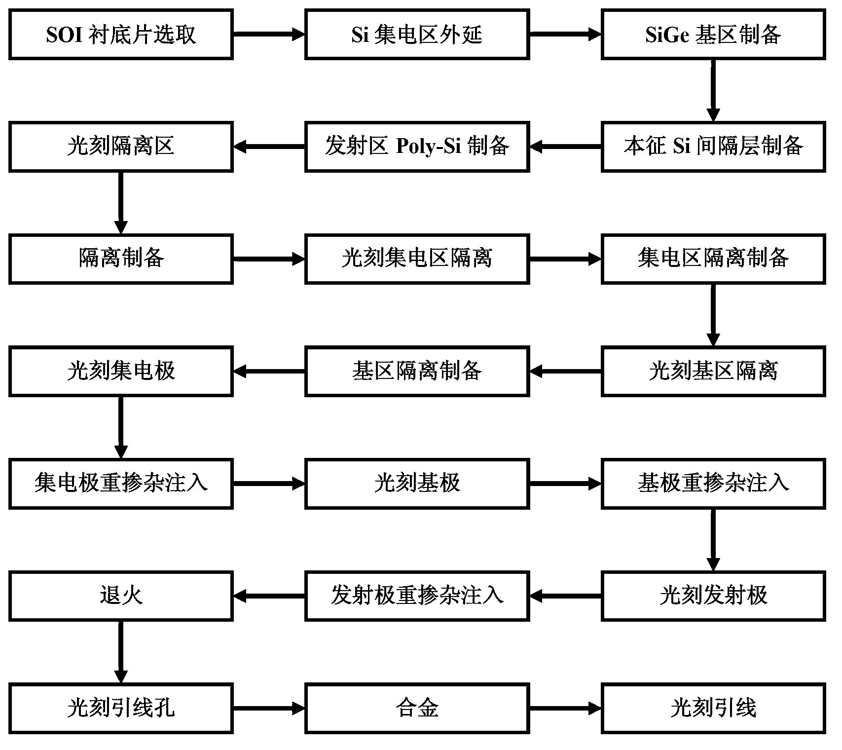
[0077] Embodiment 1: preparation of a three-polycrystalline SOI SiGe HBT planar integrated device and circuit method with a base thickness of 20nm, the specific steps are as follows:

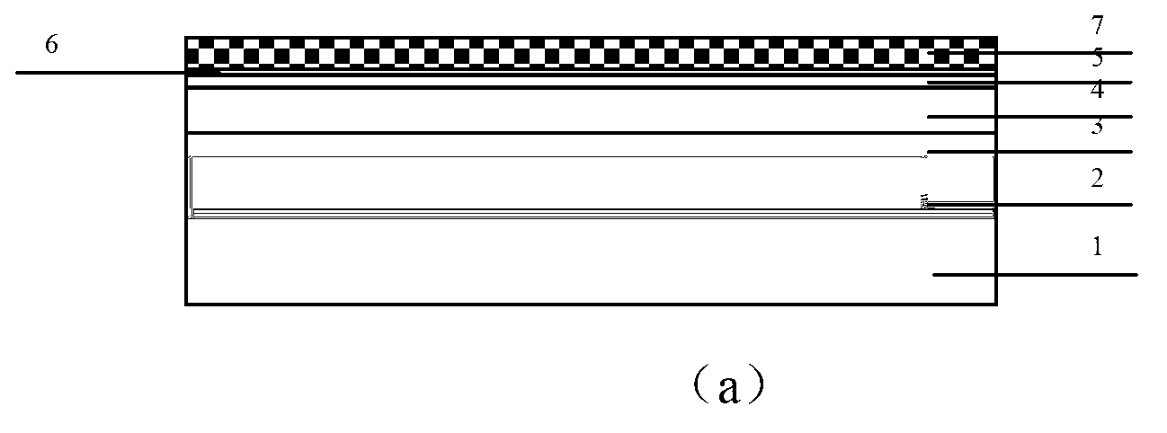
[0078] Step 1, epitaxial material preparation, such as figure 2 (a) shown.

[0079] (1a) Select an SOI substrate, the support material 1 of the lower layer of the substrate is Si, and the middle layer 2 is SiO 2 , the thickness is 150nm, and the upper layer material 3 has a doping concentration of 1×10 16 cm -3 N-type Si with a thickness of 100nm;

[0080] (1b) Using the method of chemical vapor deposition (CVD), grow a layer of N-type epitaxial Si layer 4 with a thickness of 50nm on the upper Si material at 600°C as the collector region, and the doping concentration of this layer is 1 ×10 16 cm -3 ;

[0081] (1c) Using the chemical vapor deposition (CVD) method, at 600°C, grow a layer of SiGe layer 5 with a thickness of 20nm on the substrate as the base region. The Ge composition of thi...

Embodiment 2

[0115] Embodiment 2: The preparation of a three-polycrystalline SOI SiGe HBT planar integrated device and circuit method with a base thickness of 40nm, the specific steps are as follows:

[0116] Step 1, epitaxial material preparation, such as figure 2 (a) shown.

[0117] (1a) Select an SOI substrate, the support material 1 of the lower layer of the substrate is Si, and the middle layer 2 is SiO 2 , the thickness is 300nm, and the upper material 3 has a doping concentration of 5×10 16 cm -3 N-type Si with a thickness of 120nm;

[0118] (1b) Using chemical vapor deposition (CVD), grow an N-type epitaxial Si layer 4 with a thickness of 80nm on the upper Si material at 700°C as the collector region, and the doping concentration of this layer is 5 ×10 16 cm -3 ;

[0119] (1c) Using chemical vapor deposition (CVD), grow a SiGe layer 5 with a thickness of 40nm on the substrate at 700°C. As the base region, the Ge composition of this layer is 20%, and the doping concentration...

Embodiment 3

[0153] Embodiment 3: preparation of a three-polycrystalline SOI SiGe HBT planar integrated device and circuit method with a base thickness of 60 nm, the specific steps are as follows:

[0154] Step 1, epitaxial material preparation, such as figure 2 (a) shown.

[0155] (1a) Select an SOI substrate, the support material 1 of the lower layer of the substrate is Si, and the middle layer 2 is SiO 2 , the thickness is 400nm, and the upper material 3 has a doping concentration of 1×10 17 cm -3 N-type Si with a thickness of 150nm;

[0156] (1b) Using the method of chemical vapor deposition (CVD), grow a layer of N-type epitaxial Si layer 4 with a thickness of 100 nm on the upper Si material at 750 ° C, as the collector region, and the doping concentration of this layer is 1 ×10 17 cm -3 ;

[0157] (1c) Using the chemical vapor deposition (CVD) method, at 750°C, grow a layer of SiGe layer 5 with a thickness of 60nm on the substrate, as the base region, the Ge composition of th...


PUM

PropertyMeasurementUnit
Thicknessaaaaaaaaaa
Thicknessaaaaaaaaaa
Thicknessaaaaaaaaaa

Abstract

The invention is suitable for the field of semiconductor integrated circuit, and provides a tri-polycrystal SOI (Silicon-On-Insulator) SiGe HBT (Heterojunction Bipolar Transistor) integrated device and a preparation method thereof. The preparation method comprises the following steps: continuously growing N-Si, P-SiGe, i-Si, i-Poly-Si on an SOI substrate; depositing a dielectric layer; preparing a shallow-trench isolator; photoetching a collecting zone shallow-trench isolation region; preparing a collecting zone shallow-trench isolator; etching and depositing the dielectric layer; photoetching a base region shallow-trench isolation region; preparing a base region shallow-trench isolator; photoetching a collector and implanting phosphonium ions; photoetching a base electrode and implanting boron ions; photoetching an emitter and implanting phosphonium ions; forming the contact regions of the collector, the base electrode and the emitter; and finally forming the HBT device to compose HBT integrated circuit in which the thickness of the base region is 20-60nm. The technique provided by the invention is compatible with the processing technique of the existing CMOS integrated circuit; under the condition of very few fund and equipment investments, the BiCMOS integrated device and circuit based on SOI can be prepared so that the performance of the existing analog and digital-analog hybrid integrated circuit is greatly improved.

Description

technical field [0001] The invention belongs to the field of semiconductor integrated circuits, in particular to a three-polycrystalline SOI SiGe HBT integrated device and a preparation method. Background technique [0002] Integrated circuits are the cornerstone and core of the economic development of an information society. Just as the American engineering and technology circle recently named the fifth electronic technology among the 20 greatest engineering and technological achievements in the world in the 20th century, "from vacuum tubes to semiconductors and integrated circuits, they have become the cornerstone of intelligent work in various industries today." Integrated circuits. It is one of the typical products that can best reflect the characteristics of knowledge economy. At present, the electronic information industry based on integrated circuits has become the world's largest industry. With the development of integrated circuit technology, the clear boundary be...

Claims


Application Information

Patent Timeline
IPC IPC(8): H01L29/737H01L29/08H01L21/331
Inventor 张鹤鸣周春宇宋建军胡辉勇宣荣喜王斌王海栋郝跃
Owner XIDIAN UNIV
Why Eureka
Try Eureka