Nitride high-voltage device on silicon substrate and manufacturing method thereof

A high-voltage device, nitride technology, applied in the field of microelectronics, can solve the problems of nitride epitaxial layer thickness limitation, yield reduction, lattice mismatch, etc.

Active Publication Date: 2013-02-06
ENKRIS SEMICON
View PDF5 Cites 15 Cited by
  • Summary
  • Abstract
  • Description
  • Claims
  • Application Information

AI Technical Summary

Problems solved by technology

[0007] Although the technology of growing nitride epitaxial layers on silicon materials is becoming more and more mature, the thickness of grown nitride epitaxial layers is greatly limited because of the huge lattice mismatch and thermal mismatch between silicon materials and nitrides. , Generally speaking, it is

Method used


Image

  • Nitride high-voltage device on silicon substrate and manufacturing method thereof
  • Nitride high-voltage device on silicon substrate and manufacturing method thereof
  • Nitride high-voltage device on silicon substrate and manufacturing method thereof

Examples


Embodiment Construction

[0043] The technical solution of the present invention will be introduced in detail below in conjunction with the accompanying drawings.

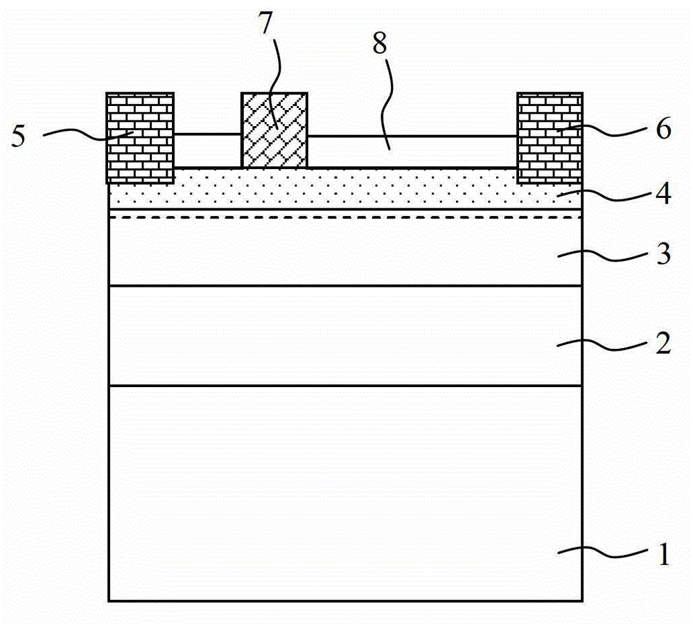
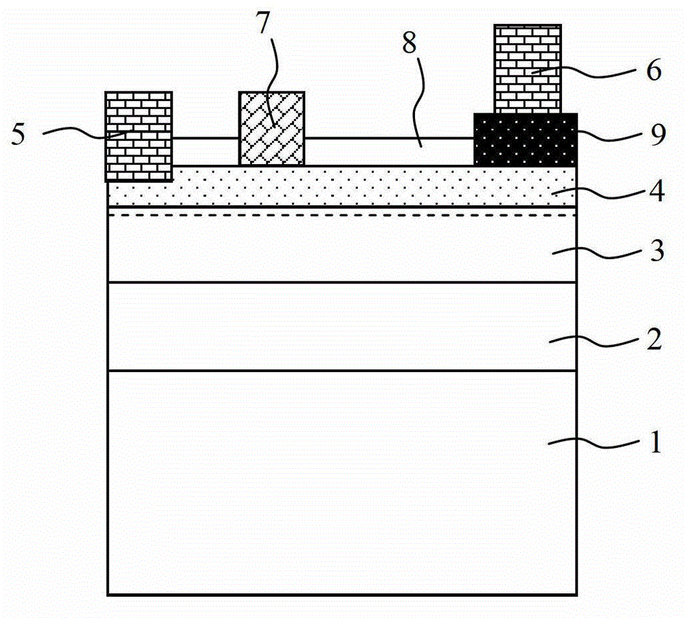
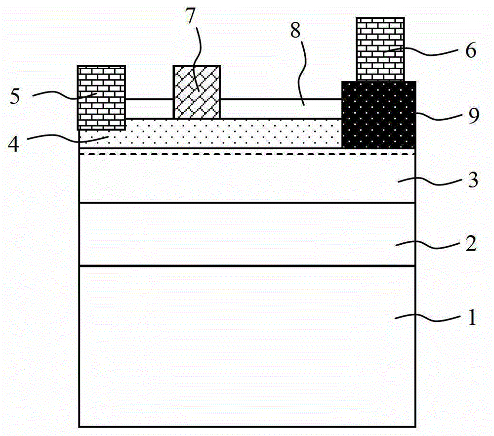
[0044] figure 1 It is a schematic diagram of the structure of a nitride device on an ordinary silicon substrate. The first layer is a single crystal silicon substrate; a buffer layer 2 is epitaxially grown on it, and the buffer layer includes GaN or AlN or other nitrides to match the substrate material and high The role of the quality epitaxial gallium nitride layer affects the crystal quality, surface morphology and electrical properties of the heterojunction composed of gallium nitride / aluminum gallium nitrogen above; the channel layer 3 is grown on the buffer layer 2, and the channel The layer includes a non-doped GaN layer; a barrier layer 4 is grown on the channel layer 3, and the barrier layer includes AlGaN or other nitrides; the channel layer 3 and the barrier layer 4 together form a semiconductor heterojunction structure, and at th...


PUM


Abstract

The invention provides a nitride high-voltage device on silicon substrate and a manufacturing method thereof. According to the nitride high-voltage device on the silicon substrate, a high-voltage tolerance layer is led into a drain electrode region, and the thickness of a partial epitaxial layer is thickened to bear higher voltage reduction, so that high punch through voltage resistant device is achieved. Via the method of partial generation, the high punch through voltage resistant device is achieved, the problems of warping and chap of nitride epitaxial layer, which are caused by a whole material with over thickness, are avoided, therefore, material generation quality is ensured, material generation efficiency is improved, and the cost is lowered.

Description

technical field [0001] The invention belongs to the technical field of microelectronics, and in particular relates to a nitride high-voltage device on a silicon substrate and a method for manufacturing the nitride high-voltage device. Background technique [0002] Wide bandgap compound semiconductor materials have shown great potential in high frequency, high temperature, high power and other fields due to their characteristics of large bandgap width, high electron saturation drift velocity, high breakdown field strength, and good thermal conductivity. Gallium nitride high electron mobility devices have attracted the attention of many researchers all over the world because of their superior performance and huge development potential. [0003] In the past, GaN power devices were made on sapphire or silicon carbide substrates. Such substrate materials are relatively expensive and difficult to achieve large-scale substrate materials and epitaxial layers, so GaN power devices ar...

Claims


Application Information

Patent Timeline
IPC IPC(8): H01L29/778H01L29/10H01L21/335
Inventor 程凯
Owner ENKRIS SEMICON
Why Eureka
Try Eureka