Zero-layer alignment mark structure for photo-etched pattern on medium substrate

A zero-layer alignment mark, medium substrate technology, which is applied in the photoengraving process, optics, instruments and other directions of the pattern surface, can solve the problems of inconvenient alignment, non-special position, easy confusion, etc., and achieves easy searching. Effect

Inactive Publication Date: 2013-02-13
THE 41ST INST OF CHINA ELECTRONICS TECH GRP
View PDF7 Cites 0 Cited by
  • Summary
  • Abstract
  • Description
  • Claims
  • Application Information

AI Technical Summary

Problems solved by technology

[0008] (1) The alignment mark is a circular through hole, and it is inconvenient to align through the handwheel movement in the X and Y directions;
[0009] (2) During photolithography alignment, since the position of the alignment mark is not special, it is difficult to search for the alignment mark, which affects work efficiency;
[0010] (3) The structure of the alignment mark is the same as that of other through-hole arrays, which is easy to confuse. Once confused, it will be reworked if it is light, and the yield will be affected if it is serious;
[0011] (4) The alignment mark is also an integral part of one or more array circuit patterns. In order to improve the yield, no matter whether the positive photolithography process or the negative photolithography process is used, the resistive film and the multilayer metal film are etched to form the circuit pattern. Before, to prevent the multi-layer thin film material deposited on the inner wall and edge of the alignment mark from being etched, it needs to be protected by manual glue filling, which adds an additional process

Method used


Image

  • Zero-layer alignment mark structure for photo-etched pattern on medium substrate
  • Zero-layer alignment mark structure for photo-etched pattern on medium substrate
  • Zero-layer alignment mark structure for photo-etched pattern on medium substrate

Examples


Embodiment 1

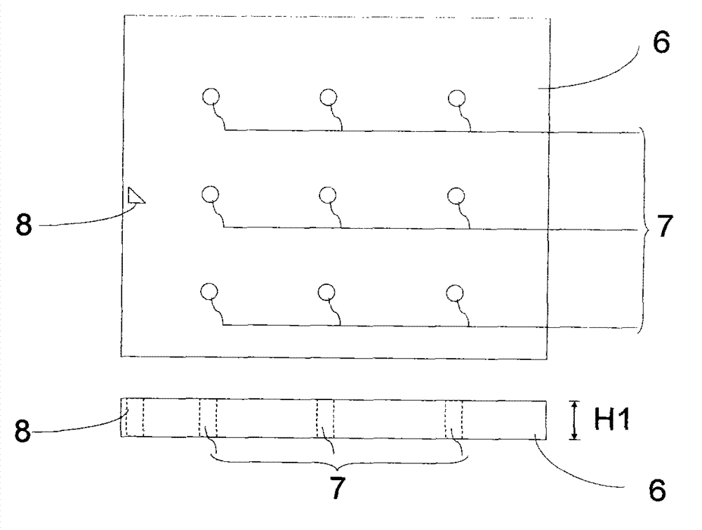
[0030] see figure 2 , the zero-layer alignment mark structure 8 is a longitudinal through hole arranged at the edge of the dielectric substrate 6 and it is a right triangle. In this embodiment, the dielectric substrate 6 where the zero-layer alignment mark structure 8 is located is made of alumina ceramics with a purity of more than 99.6%, the plane size is 50.8mm x 50.8mm, and the thickness H1 is 0.635mm.

Embodiment 2

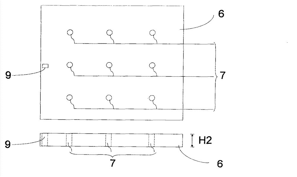
[0032] see image 3 , the zero-layer alignment mark structure 9 is a longitudinal through hole disposed at the edge of the dielectric substrate 6 and is a rectangle. In this embodiment, the dielectric substrate 6 where the zero-layer alignment mark structure 9 is located is made of alumina ceramics with a purity of more than 99.6%, the plane size is 50.8mm×50.8mm, and the thickness H2 is 0.254mm.

Embodiment 3

[0034] see Figure 4 , the zero-layer alignment mark structure 10 is a longitudinal through hole disposed on the edge of the dielectric substrate 6 and is a right-angled trapezoid. In this embodiment, the dielectric substrate 6 where the zero-layer alignment mark structure 10 is located is made of sapphire, has a plane size of 50.8 mm×50.8 mm, and a thickness H3 of 0.508 mm.

[0035] In the fabrication process of microwave thin film hybrid integrated circuit, use Figure 2 to Figure 4 The zero-layer alignment mark structures 8, 9, 10 described in can ensure that the microwave thin film hybrid integrated circuit on the dielectric substrate is manufactured at its preset position.

[0036] In summary, a zero-layer alignment mark structure for photolithographic patterns on a dielectric substrate according to the present invention is a right-angled longitudinal through hole arranged at the edge of the dielectric substrate, which can ensure that the micro-array metallization The a...


PUM

PropertyMeasurementUnit
thicknessaaaaaaaaaa
sizeaaaaaaaaaa
thicknessaaaaaaaaaa

Abstract

The invention discloses a zero-layer alignment mark structure for a photo-etched pattern on a medium substrate. The zero-layer alignment mark structure is a right-angle longitudinal through hole formed in the edge of the medium substrate. The zero-layer alignment mark structure for the medium substrate can be a right triangle, a rectangle or a right trapezoid; the medium substrate on which the zero-layer alignment mark structure is arranged comprises an aluminum oxide ceramic with purity of more than 99.6% and a sapphire; and the medium substrate is 0.1-0.65mm in thickness. By adopting the alignment mark structure, alignment accuracy of a photo-etched film resistor and a metal conduction band pattern on the medium substrate with a micro array metalized through hole can be guaranteed and yield of a microwave film integrated circuit can be also increased.

Description

technical field [0001] The invention relates to a zero-layer alignment mark structure used for photolithography patterns on a dielectric substrate, in particular to an alignment mark related to photolithography devices in the field of microwave thin film hybrid integrated circuits or other micro-device manufacturing. Background technique [0002] In the microwave frequency band, more circuits need to be grounded directly, and metallization of tiny through holes is a good grounding method. Its purpose is to reduce the grounding inductance and shorten the heat transfer channel, which is especially important for microwave and millimeter wave device and circuit design. Therefore, tiny metallized vias have become a common passive component for microwave and millimeter wave integrated circuits, and the vias are usually circular in shape. [0003] The requirements for the selection of metal materials for the surface coating layer of microwave thin film hybrid integrated circuits i...

Claims


Application Information

Patent Timeline
Patent Type & Authority Applications(China)
IPC IPC(8): G03F9/00
Inventor 曹乾涛
Owner THE 41ST INST OF CHINA ELECTRONICS TECH GRP
Why Eureka
Try Eureka