Method for forming first copper metal layer
A technology of copper metal and bottom layer, which is applied in the field of forming the first copper metal layer, can solve the problems affecting the performance and stability of the device, the thickness difference of the remaining dielectric layer 131 is large, and the control is difficult, so as to achieve the effect of improving performance and stability
- Summary
- Abstract
- Description
- Claims
- Application Information
AI Technical Summary
Problems solved by technology
Method used
Image

Examples
Embodiment Construction
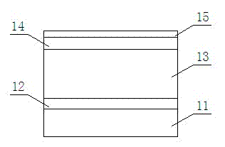
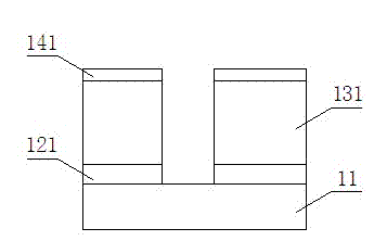
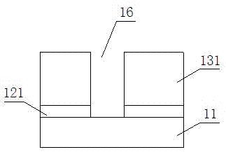
[0019] Figure 6-11 It is a schematic structural diagram of the process flow of the method for forming the first copper metal layer in the present invention;
[0020] like Figure 6-11 As shown, firstly, on the silicon wafer 21 having the underlying device structure, an etch barrier layer 22 made of silicon nitride (SiN) or nitrogen-doped silicon carbide (NDC) is sequentially deposited from bottom to top, and the material is made of dioxide Silicon (SiO 2 ) or a carbon-doped silicon dioxide dielectric layer 23, a hard mask layer 24 made of amorphous carbon (amorphous carbon) and a dielectric anti-reflection layer (DARC) 25, spin-coating photoresist to cover the dielectric anti-reflection layer The upper surface of the reflective layer 25 is exposed and developed to remove excess photoresist to form a photoresist 3, and use the photoresist as grinding to etch back the medium antireflection layer 25, hard mask layer 24, dielectric layer 23 and After the barrier layer 22 is et...
PUM
 Abstract
Description
Claims
Application Information
 - R&D Engineer
- R&D Manager
- IP Professional
- Industry Leading Data Capabilities
- Powerful AI technology
- Patent DNA Extraction
Browse by: Latest US Patents, China's latest patents, Technical Efficacy Thesaurus, Application Domain, Technology Topic.
© 2024 PatSnap. All rights reserved.Legal|Privacy policy|Modern Slavery Act Transparency Statement|Sitemap