Transparent back film for solar cell
A solar cell and transparent technology, applied in circuits, photovoltaic power generation, electrical components, etc., can solve the problems of complex production process of fluoropolymers, environmental pollution in the production process, easy to fall off, etc., to avoid falling off and delamination, overcome the The light transmittance will be significantly reduced and the bond strength will be improved
- Summary
- Abstract
- Description
- Claims
- Application Information
AI Technical Summary
Problems solved by technology
Method used
Image
Examples
Embodiment 1
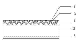
[0031] Such as figure 1 As shown, the back film of the present invention includes an electrical insulation layer 3 , an adhesive layer 2 and a weather-resistant layer 1 located outside the electrical insulation layer, and an adhesive layer 4 located inside the electrical insulation layer 3 . The electrical insulating layer 3 of the present invention is a transparent PET with a thickness of 0.250mm, and the outer side of the electrical insulating layer is coated with an adhesive layer 2, and the adhesive layer 2 is a transparent two-component polyurethane adhesive with a thickness of 0.008mm The weather-resistant layer 1 is a transparent weather-resistant PET with a thickness of 0.050mm, and an adhesive layer 4 is coated on the inside of the electrical insulating layer 3, and the adhesive layer 4 is a transparent one-component acrylic resin with a thickness of 0.006mm.
[0032] The production method is to apply the adhesive layer 4 on one side of the electrical insulating layer...
Embodiment 2
[0034] Such as figure 1 As shown, the electrical insulating layer 3 of the back film of the present invention is a transparent PEN with a thickness of 0.350mm, and the outer side of the electrical insulating layer is coated with an adhesive layer 2, and the adhesive layer 2 is a transparent double-pack with a thickness of 0.020mm. Polyurethane adhesive, the weather-resistant layer 1 is a transparent weather-resistant PET with a thickness of 0.025mm, and an adhesive layer 4 is coated on the inside of the electrical insulation layer 3, and the adhesive layer 4 is a transparent two-component layer with a thickness of 0.002mm Acrylic.
[0035] of the present invention The production method is as follows: on one side of the electrical insulating layer 3, the adhesive layer 4 is coated by the gravure coating method, and the coating speed is 40m / min. One side is coated with the adhesive layer 2 by the gravure coating method, the coating speed is 15 m / min, after drying at 80°C, the...
Embodiment 3
[0037] Such as figure 1 As shown, the electrical insulating layer 3 of the present invention is a transparent PETG with a thickness of 0.125 mm, and the outer side of the electrical insulating layer is coated with an adhesive layer 2, and the adhesive layer 2 is a transparent one-component polyurethane with a thickness of 0.004 mm. Adhesive, the weather-resistant layer 1 is a transparent weather-resistant PET with a thickness of 0.175mm, and an adhesive layer 4 is coated on the inside of the electrical insulating layer 3, and the adhesive layer 4 is a transparent one-component acrylic resin with a thickness of 0.015mm .
[0038] of the present invention The production method is as follows: on one side of the electrical insulating layer 3, the adhesive layer 4 is coated by the gravure coating method, the coating speed is 70m / min, and it is wound after drying at 110°C. One side is coated with the adhesive layer 2 by the gravure coating method, the coating speed is 60 m / min, a...
PUM
| Property | Measurement | Unit |
|---|---|---|
| thickness | aaaaa | aaaaa |
| thickness | aaaaa | aaaaa |
| thickness | aaaaa | aaaaa |
Abstract
Description
Claims
Application Information


