Method for manufacturing trench gate type IGBT (insulated gate bipolar transistor) chip

A fabrication method and trench gate technology, applied in semiconductor/solid-state device manufacturing, electrical components, circuits, etc., can solve problems such as single hole blocking effect

Active Publication Date: 2013-02-27
ZHUZHOU CRRC TIMES SEMICON CO LTD
View PDF4 Cites 11 Cited by
  • Summary
  • Abstract
  • Description
  • Claims
  • Application Information

AI Technical Summary

Problems solved by technology

[0006] The various technologies mentioned above have enhanced the conductance modulation effect of the IGBT to a certain extent, thereby reducing the conduc

Method used


Image

  • Method for manufacturing trench gate type IGBT (insulated gate bipolar transistor) chip
  • Method for manufacturing trench gate type IGBT (insulated gate bipolar transistor) chip
  • Method for manufacturing trench gate type IGBT (insulated gate bipolar transistor) chip

Examples


Example Embodiment

[0182] The technical solutions in the embodiments of the present invention will be clearly and completely described below in conjunction with the accompanying drawings in the embodiments of the present invention. Obviously, the described embodiments are only a part of the embodiments of the present invention, rather than all the embodiments. Based on the embodiments of the present invention, all other embodiments obtained by those of ordinary skill in the art without creative work shall fall within the protection scope of the present invention.
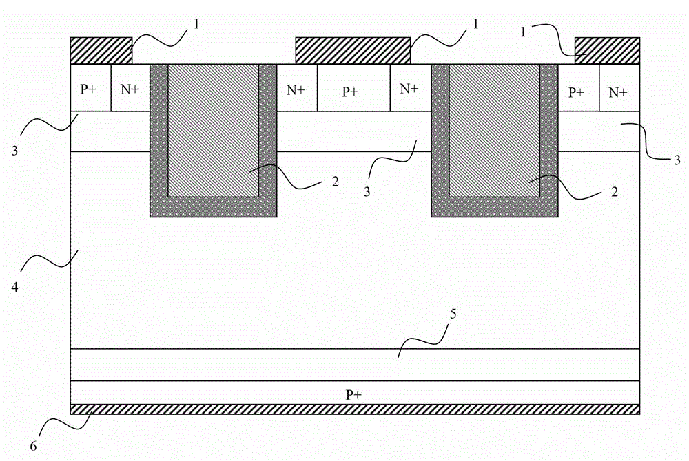
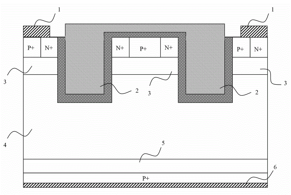
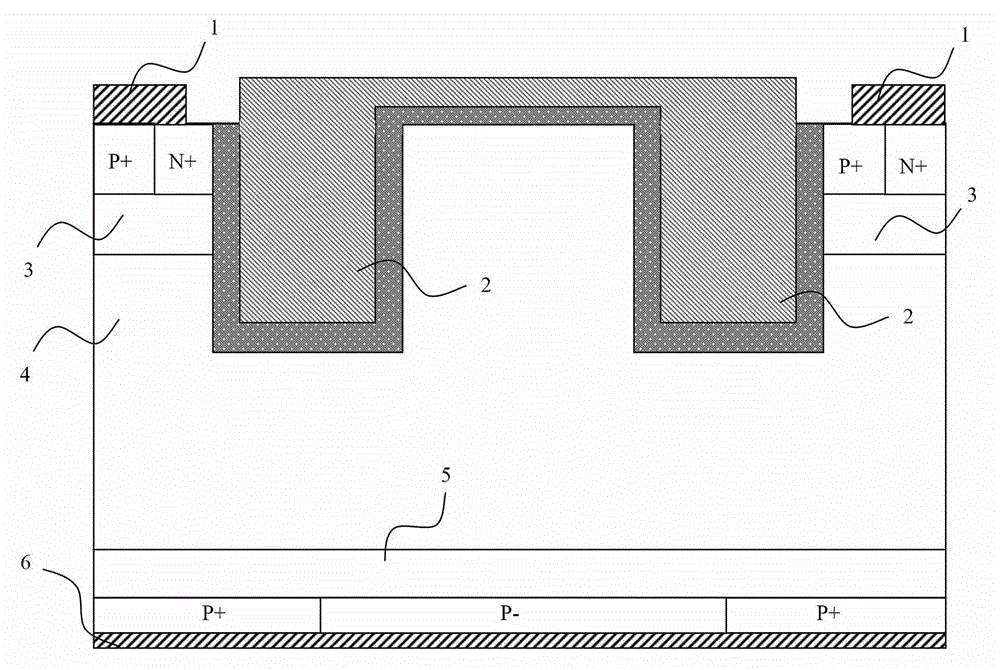
[0183] As attached Figure 4 Attached Figure 52 As shown, specific embodiments of a trench gate IGBT chip manufacturing method of the present invention and a trench gate IGBT chip manufactured according to the trench gate IGBT chip manufacturing method of the present invention are given. The following is combined with the drawings and The specific embodiments further illustrate the present invention.

[0184] As attached Figure 4 Attach...


PUM

PropertyMeasurementUnit
Thicknessaaaaaaaaaa
Thicknessaaaaaaaaaa

Abstract

The invention discloses a method for manufacturing a trench gate type IGBT (insulated gate bipolar transistor) chip, which comprises the following steps: selecting two N-shaped semiconductor substrates, and carrying out oxidation or deposition on one of the substrates, so that insulating materials including silicon oxides or nitric oxides are formed on the surface of the substrate; carrying out photoetching and etching on the insulating materials on the surface of the substrate so as to form a dielectric buried layer; carrying out photoetching and etching on the other substrates so as to form a figure coincided with the concave-convex surface of the dielectric buried layer; carrying out concave-convex surface butt-joint on the dielectric buried layer and the figure, and bonding the two substrates together at high temperature; according to voltage-withstanding requirements and machining allowances, respectively carrying out thinning processing on the two substrates, and controlling the dielectric buried layer at a design depth, so that a chip manufacturing intermediate is formed; and completing the manufacturing process of a trench gate type IGBT chip. According to the invention, the drop voltage of the chip is reduced, a compromising relation with shut-off loss is optimized, and the lower power consumption is realized, thereby improving the power density, operating junction temperature and reliability of the IGBT chip.

Description

technical field [0001] The invention relates to a semiconductor IGBT (Insulted Gate Bipolar Transistor, insulated gate bipolar transistor) chip structure, in particular to a trench gate IGBT chip structure with double hole blocking effects. Background technique [0002] Insulated gate bipolar transistor (IGBT) has the characteristics of on-state voltage drop, large current capacity, high input impedance, fast response and simple control, and is widely used in industry, information, new energy, medicine, transportation, military and aviation fields . In order to reduce the turn-on voltage drop of the IGBT, people use a trench gate structure to change the channel from horizontal to vertical, eliminating the influence of RJFET in the on-resistance. At the same time, the cell size is reduced, the cell density is greatly increased, the total channel width of each chip is increased, and the channel resistance is reduced. On the other hand, since the polysilicon gate area increas...

Claims


Application Information

Patent Timeline
IPC IPC(8): H01L21/331
Inventor 刘国友覃荣震黄建伟
Owner ZHUZHOU CRRC TIMES SEMICON CO LTD
Why Eureka
Try Eureka