
Method for manufacturing mask read-only memory

A manufacturing method and mask read-only technology, which is applied in semiconductor/solid-state device manufacturing, electrical components, circuits, etc., can solve the problems of transistor work function and feature size that cannot form resistance, etc.

Inactive Publication Date: 2013-02-27
SHANGHAI HUAHONG GRACE SEMICON MFG CORP
View PDF5 Cites 1 Cited by
  • Summary
  • Abstract
  • Description
  • Claims
  • Application Information

AI Technical Summary

Problems solved by technology

[0006] The invention provides a method for manufacturing a masked read-only memory. The method for manufacturing a masked read-only memory uses an undoped gate material layer to form a gate, and selectively forms metal silicide on the gate , such a process has good compatibility with the logic process, etc., and overcomes the influence of the use of gate oxide layer, doped polysilicon, and tungsten silicide gate on the work function and feature size of the transistor and the inability to form devices such as resistors. question

Method used


Image

  • Method for manufacturing mask read-only memory
  • Method for manufacturing mask read-only memory
  • Method for manufacturing mask read-only memory

Examples


Embodiment Construction

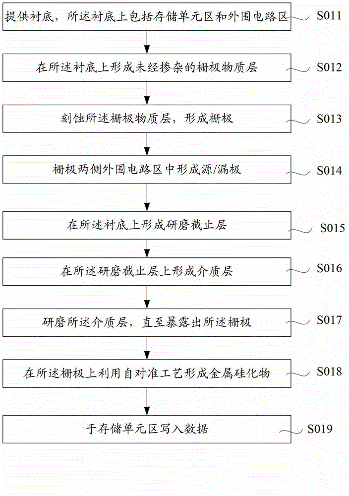
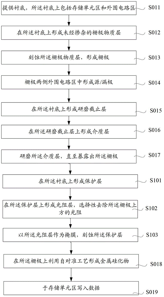
[0039] As mentioned in the background art, the existing manufacturing method of the mask ROM has the problem of incompatibility with the logic process. Therefore, the present invention provides a method for manufacturing a masked read-only memory, using an undoped gate material layer to form a gate, and forming a metal silicide on the gate. Such a process has a good relationship with logic processes. The compatibility solves the problem that the use of doped polysilicon and tungsten silicide gates affects the work function and feature size of transistors and the problems that devices such as resistors cannot be formed.

[0040] The present invention will be described in more detail below with reference to the accompanying drawings, wherein preferred embodiments of the present invention are shown, it should be understood that those skilled in the art can modify the present invention described herein and still achieve the advantageous effects of the present invention. Therefore,...


PUM

PropertyMeasurementUnit
Thicknessaaaaaaaaaa
Thicknessaaaaaaaaaa
Thicknessaaaaaaaaaa

Abstract

The invention provides a method for manufacturing a mask read-only memory. The method comprises the following steps of: providing a substrate, wherein a storage unit area and a peripheral circuit area are defined on the substrate; forming an undoped gate substance layer on the substrate; etching the gate substance layer, and forming a gate; performing shallow doping ion implantation in the peripheral circuit area; forming side walls on two sides of the gate and a resistor; performing heavy doping ion implantation in the peripheral circuit area; forming a grinding cut-off layer on the substrate; forming a dielectric layer on the grinding cut-off layer; grinding the dielectric layer until the gate is exposed; forming a metal silicide on the gate by utilizing a self-aligned process; and writing data in the storage unit area. The method does not have adverse effects on the work function of a transistor and feature size of a photolithography process, a resistor and other devices can be formed in the peripheral circuit area, and the method has high compatibility with a logic process and the like.

Description

technical field [0001] The invention relates to the technical field of integrated circuit manufacturing, in particular to a method for manufacturing a mask read-only memory. Background technique [0002] Mask read-only memory (MROM) is one of the common types of semiconductor memory, which is widely used in electronic products such as computers. The mask read-only memory is composed of a memory cell array and peripheral logic circuits, and the memory cell array is often composed of mutually orthogonal bit lines and word lines. Peripheral logic circuits often include devices such as logic transistors. [0003] Generally, the process flow of making a mask read-only memory is as follows: a shallow trench isolation structure is formed on a semiconductor substrate; an ion implantation process is performed on the peripheral circuit area of ​​the semiconductor substrate to form a well area, and ion implantation is performed on the area defined as a memory cell Forming a bit line;...

Claims


Application Information

Patent Timeline
IPC IPC(8): H01L21/8246
Inventor 于涛
Owner SHANGHAI HUAHONG GRACE SEMICON MFG CORP
Learn More