Treatment method of Si-Si bonded surface stains

A technology for surface contamination and treatment methods, which is applied in the direction of processing microstructure devices, photolithography on patterned surfaces, precision positioning equipment, etc., can solve problems such as ion contamination, and achieve the purpose of avoiding contamination, improving integrity, and processing The effect of simple method

Active Publication Date: 2013-03-13
EAST CHINA INST OF OPTOELECTRONICS INTEGRATEDDEVICE
View PDF4 Cites 2 Cited by
  • Summary
  • Abstract
  • Description
  • Claims
  • Application Information

AI Technical Summary

Problems solved by technology

[0005] The purpose of the present invention is to solve the problem of solid particles and ion contamination on the surface of silicon wafers when silicon-silicon is directly bonded, and to provide a method for treating surface contamination of silicon-silicon bonding

Method used


Image

  • Treatment method of Si-Si bonded surface stains
  • Treatment method of Si-Si bonded surface stains

Examples


Embodiment Construction

[0022] A method for treating contamination of a silicon-silicon bonding surface provided by the present invention will be further described below in conjunction with the accompanying drawings.

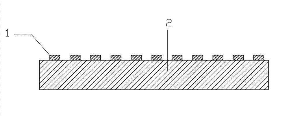
[0023] 1. Silicon gasket structure and production:

[0024] like figure 1 As shown, the silicon spacer among the present invention comprises: making silicon nitride 1 thin film on the surface of monocrystalline silicon wafer 2, the manufacturing process of silicon nitride thin film is known technology, mainly contains the following several steps:

[0025] (a) Routine cleaning of silicon wafers;

[0026] (b) PECVD deposits a layer of 1500? silicon nitride film;

[0027] (c) LC100A photoresist photolithographic pattern;

[0028] (d) Dry etching silicon nitride to form silicon nitride bumps 2 in an array on the single crystal silicon wafer 2 .

[0029] 2. Cut the silicon gasket with a dicing machine so that the silicon gasket is adapted to the shape of the silicon wafer to be bonded; ...


PUM


Abstract

The invention relates to a treatment method of Si-Si bonded surface stains. The method comprises the steps of: a. making a silicon gasket matching a to-be-bonded silicon wafer in shape, and depositing a layer of silicon nitride film on the silicone gasket surface; b. aligning the silicon nitride deposited side of the silicon gasket with the to-be-bonded silicon wafer to stick them tightly, and putting them in a bonding jig for fixation; c. pre-bonding the silicon gasket and the to-be-bonded silicon wafer, and then tearing off the silicon gasket; and d. subjecting the pre-bonded silicon wafer to sintering bonding . The invention has the advantages that: (1) no chemical and physical removal means is needed, the integrity of the movable structure of an MEMS device can be improved; and (2) being simple and practicable, the method is easy to operate, and is suitable for wide application in production and processing.

Description

[0001] technical field [0002] The invention belongs to the technical field of micro-electronic machinery, and relates to a method for treating contamination on the surface of silicon-silicon directly bonded silicon wafers. Background technique [0003] Silicon-silicon direct bonding technology is a typical MEMS bonding technology. It is two CMP-polished silicon wafers after surface cleaning and activation treatment, directly bonded at room temperature, pre-bonded at low temperature, and then subjected to high temperature bonding. Annealing is a bonding technique that increases bond strength. This bonding technology does not require adhesives, the resistivity and conductivity type of the two bonding sheets can be freely selected, and because of the bonding of the same material, there is no residual stress after bonding, and this bonding seal Excellent bonding performance, no need to add getters for ordinary vacuum packaging, therefore, this bonding technology has attracted...

Claims


Application Information

Patent Timeline
Patent Type & Authority Applications(China)
IPC IPC(8): B81C3/00
Inventor 陈博郭群英徐栋黄斌何凯旋陈璞王文婧王鹏汪祖民
Owner EAST CHINA INST OF OPTOELECTRONICS INTEGRATEDDEVICE
Why Eureka
Try Eureka