Illumination stability amorphous metallic oxide thin film transistor (TFT) device and display device

An amorphous and oxide technology, applied in semiconductor/solid-state device components, semiconductor/solid-state device manufacturing, semiconductor devices, etc., to reduce surface damage and improve long-term stability

Active Publication Date: 2013-03-13
INST OF MICROELECTRONICS CHINESE ACAD OF SCI
View PDF8 Cites 38 Cited by
  • Summary
  • Abstract
  • Description
  • Claims
  • Application Information

AI Technical Summary

Problems solved by technology

[0009] Therefore, the technical problem to be solved by the present invention is to overcome the initial stability, long-term bias electric stress stability and light exposure of the existing inverted gate BCE, or inverted gate ESL, or coplanar inverted gate amorphous oxide thin film transistors. A series of problems such as long-term bias electric stress stability, etc., provide a new type of high-efficiency and low-cost stable drive AMOLED or AMLCD display amorphous oxide TFT device structure

Method used


Image

  • Illumination stability amorphous metallic oxide thin film transistor (TFT) device and display device
  • Illumination stability amorphous metallic oxide thin film transistor (TFT) device and display device
  • Illumination stability amorphous metallic oxide thin film transistor (TFT) device and display device

Examples


Embodiment Construction

[0041] The features and technical effects of the technical solution of the present invention will be described in detail below with reference to the accompanying drawings and in combination with schematic embodiments, and a high-stability amorphous metal oxide transistor device structure and its preparation method are disclosed. It should be pointed out that similar reference numerals represent similar structures, and the terms "first", "second", "upper", "lower" and the like used in this application can be used to modify various device structures. These modifications do not imply a spatial, sequential or hierarchical relationship of the modified device structures unless specifically stated.

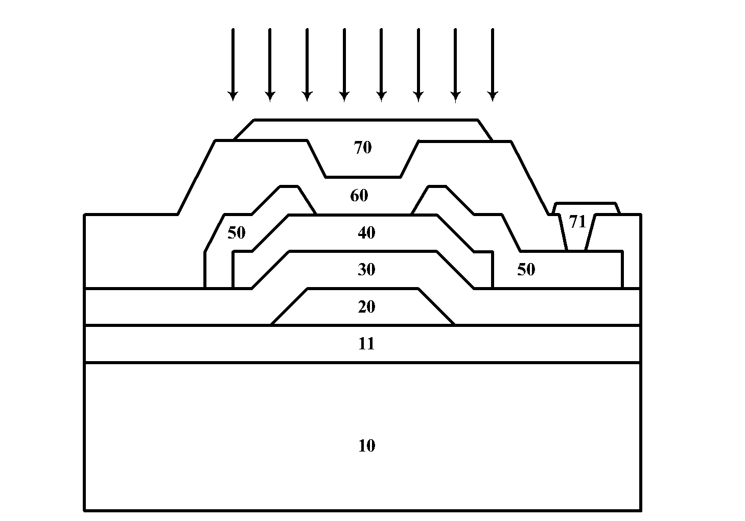
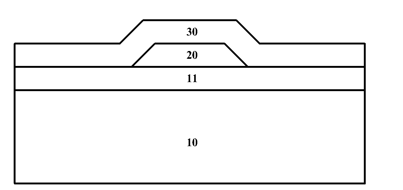
[0042] Such as figure 1 Shown is a schematic cross-sectional view of an amorphous oxide TFT with a top gate protection electrode according to the present invention, including a substrate 10, a buffer layer 11 on the substrate 10, an inverted gate electrode 20 on the buffer layer 11, and ...


PUM

PropertyMeasurementUnit
thicknessaaaaaaaaaa

Abstract

The invention provides an illumination stability amorphous metallic oxide thin film transistor (TFT) device which comprises a substrate, a reverse gate electrode, a gate insulating medium layer, a channel layer formed by amorphous metallic oxide, a source electrode and drain electrode, a passivation layer and a driving electrode which penetrates through the passivation layer to be contacted with the source electrode and drain electrode. The illumination stability amorphous metallic oxide TFT device is characterized in that a top gate protective electrode capable of greatly absorbing ultraviolet light is further arranged on the top portion of the passivation layer. By means of the TFT device, a transparent conducting material capable of greatly absorbing ultraviolet light is formed on the top portion of an active area of the device to effectively filter environment and reduce conductive influences of the ultraviolet light of an active light source on a channel, long-term stability of the device is improved, simultaneously electrostatic potential produced by consumption difference of the top gate protective electrode is used for repelling electric conduction charge of a back channel, surface damage of the back channel is weakened, and influences of defects on the long-term stability of the device are reduced. Simultaneously, an indium tin oxide (ITO) top gate electrode and an ITO lower electrode for driving organic light emitting diode share one layer of Mask, and no extra additional material electrode and imaging technology exist.

Description

technical field [0001] The invention relates to a semiconductor device, in particular to a device structure of an amorphous metal oxide thin film transistor (TFT) with high stability under light and a display device using the TFT, belonging to the technology of flat panel display devices. Background technique [0002] Active-Matrix Organic Light Emitting Diodes (AMOLED) displays have excellent characteristics such as short response time for moving images, bright colors, high contrast, wide viewing angles, low power consumption, ultra-light and ultra-thin, and are considered to replace The active liquid crystal display (AMLCD), which currently occupies a mainstream position, has become the core technology platform of the next generation mainstream display. The successful development of high-resolution and mainstream-sized AMOLED display panels mainly involves three technical research fields: the performance of TFT drive substrates, the characteristics of OLED materials, and t...

Claims


Application Information

Patent Timeline
Patent Type & Authority Applications(China)
IPC IPC(8): H01L29/786H01L23/552H01L29/40H01L21/77
Inventor 殷华湘王玉光董立军陈大鹏
Owner INST OF MICROELECTRONICS CHINESE ACAD OF SCI
Why Eureka
Try Eureka