Transparent conductive film layer for capacitive touch screen

A capacitive touch screen, transparent conductive film technology, applied to the conductive layer on the insulating carrier, cable/conductor manufacturing, circuit and other directions, can solve the problems of expensive ITO film, difficult to protect, fall off, etc., to improve product yield and reliability Sexuality, avoid easy falling off and damage, reduce production cost

Inactive Publication Date: 2013-03-20
无锡力合光电石墨烯应用研发中心有限公司 +1
View PDF8 Cites 16 Cited by
  • Summary
  • Abstract
  • Description
  • Claims
  • Application Information

AI Technical Summary

Problems solved by technology

[0007] Although the ITO film produced by the existing process has high conductivity and transparency, which can basically meet the needs of some electronic products for these two technical indicators, there are still many difficulties that are difficult to overcome:
[0008] (1) ITO is very brittle and brittle, so it is easy to be worn during application or cracks and falls off during bending, which affects the service life
[0009] (2) After the ITO film is formed, high temperature treatment is required to achieve high conductivity. When using a plastic substrate, due to the limited processing temperature, the conductivity and transparency of the film are low
[0010] (3) Affected by raw materials, production equipment and processes, ITO thin films will become more and more expensive
[0016] (2) The hue of graphene is completely colorless
[0022] (1) The matching of conductivity and transparency of alternative transparent conductive oxide TCO film layers (such as AZO, FTO, etc.) has not yet reached the indicators used in the display industry such as touch screen products, such as a resistivity of 10 -4 On the order of Ω·cm, the average transmittance of visible light Tavg> 80%;
[0023] (2) TCC (transparent conductive film) films based on nanomaterials, such as graphene films, have disadvantages such as poor adhesion and difficult protection

Method used


Image

  • Transparent conductive film layer for capacitive touch screen
  • Transparent conductive film layer for capacitive touch screen
  • Transparent conductive film layer for capacitive touch screen

Examples


Embodiment 1

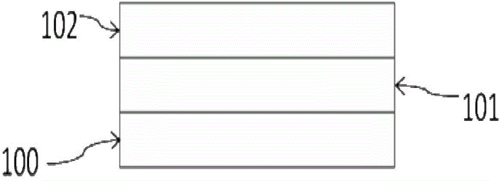
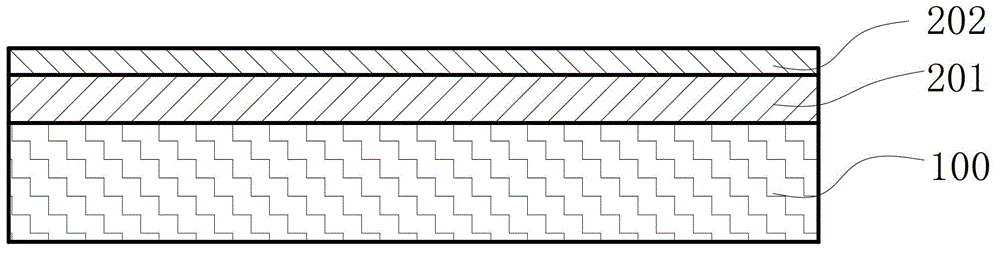
[0077] A transparent conductive film layer for a capacitive touch screen, comprising a substrate 100, a graphene transparent conductive layer 201 attached to the substrate, and a transparent conductive oxide film layer 202 deposited on the graphene material;

[0078] Wherein, the thickness of the graphene transparent conductive layer 201 is 0.3nm; the graphene transparent conductive layer 201 is a monoatomic layer; the optical transmittance of the visible light of the graphene transparent conductive layer 201 is 95%;

[0079] The transparent conductive oxide film layer 202 is an AZO film with a thickness of 100 nm; the substrate 100 is a glass substrate with a thickness of 1 mm; image 3 It is a schematic structural view of the transparent conductive film layer used in the capacitive touch screen described in Embodiment 1.

[0080] Preparation

[0081] The preparation method of the transparent conductive film layer of the capacitive touch screen comprises:

[0082] (1) Using...

Embodiment 2

[0087] A transparent conductive film layer for a capacitive touch screen, comprising a substrate 100, a graphene transparent conductive layer 201 attached to the substrate, and a transparent conductive oxide film layer 202 deposited on the graphene material;

[0088] Wherein, the thickness of the graphene transparent conductive layer 201 is 1 nm; the number of atomic layers of the graphene transparent conductive layer 201 is 3 layers; the optical transmittance of visible light of the graphene transparent conductive layer 201 is ≥ 89%;

[0089] The transparent conductive oxide film layer 202 is an AZO thin film with a thickness of 100 nm; the substrate 100 is a glass substrate with a thickness of 2 mm.

[0090] Preparation

[0091] A preparation method of a transparent conductive film layer of a capacitive touch screen, comprising:

[0092] (1) Using the method disclosed in CN102220566A to prepare a graphene film, specifically: placing the metal substrate in a vacuum tube furn...

Embodiment 3

[0097] A transparent conductive film layer for a capacitive touch screen, comprising a substrate 100, a graphene transparent conductive layer 201 attached to the substrate, and a transparent conductive oxide film layer 202 deposited on the graphene material;

[0098] Wherein, the thickness of the graphene transparent conductive layer 201 is 1.5nm; the number of atomic layers of the graphene transparent conductive layer 201 is 5 layers; the optical transmittance of the visible light of the graphene transparent conductive layer 201 is ≥ 87%;

[0099] The transparent conductive oxide film layer 202 is an FTO film with a thickness of 100 nm; the substrate 100 is a glass substrate with a thickness of 0.3 mm.

[0100] Preparation

[0101] A preparation method of a transparent conductive film layer of a capacitive touch screen, comprising:

[0102] (1) Using the method disclosed in CN102220566A to prepare a graphene film, specifically: placing the metal substrate in a vacuum tube fu...


PUM

PropertyMeasurementUnit
thicknessaaaaaaaaaa
thicknessaaaaaaaaaa
thicknessaaaaaaaaaa

Abstract

The utility model relates to a transparent conductive film layer for a capacitive touch screen. The transparent conductive film layer comprises a substrate (100), a graphene transparent conductive layer (201) attached on the substrate and a transparent conductive oxide film layer (202) deposited on graphene materials. The transparent conductive film layer is good in conductive performance, high in visible light transmittance and good in adhesive force; and materials are easy to obtain, the cost is low, the technological process is simple, and the whole product yield of the manufactured capacitive touch screen is high.

Description

technical field [0001] The present invention relates to a transparent conductive film layer, in particular to a transparent conductive film layer for a capacitive touch screen, in particular to a method for preparing a graphene-based conductive material and a transparent conductive protective film layer for a touch screen product and The technology belongs to the technical field of touch screen. Background technique [0002] Transparent conductive films are essential components for the production of liquid crystal displays, OLED displays, thin-film solar cells, touch screens, electromagnetic shielding, and more. In recent years, with the development of information technology and products, the market demand for transparent conductive films is increasing. The transparent conductive film refers to: ① high transmittance to visible light (the wavelength λ is in the range of 380-760nm), and the average light transmittance Tavg of visible light is > 80%; ② high electrical condu...

Claims


Application Information

Patent Timeline
Patent Type & Authority Applications(China)
IPC IPC(8): H01B5/14H01B1/04H01B13/00
Inventor 刘志斌黄海东吴勇熊维龙赵斌
Owner 无锡力合光电石墨烯应用研发中心有限公司
Why Eureka
Try Eureka