
Ceramic via substrate, metallized ceramic via substrate, and method for manufacturing both

一种通孔基板、陶瓷的技术,应用在印刷电路制造、金属花纹材料、电气元件等方向,能够解决生产率下降、不是制造金属化通孔基板、难以形成致密的通孔等问题,达到密合性良好的效果

Active Publication Date: 2013-03-20
TOKUYAMA CORP
View PDF6 Cites 7 Cited by
  • Summary
  • Abstract
  • Description
  • Claims
  • Application Information

AI Technical Summary

Problems solved by technology

[0007] However, since the metal paste itself shrinks, the metal paste in the through-hole shrinks when sintered, and voids are generated in the formed conductive via, making it difficult to form a dense via.
[0008] Patent Document 1 uses sputtering to form a titanium layer and a copper layer on a ceramic substrate with a through hole, and then forms a wiring pattern and a conductive via hole by copper plating. Since the sputtering process is necessary in this method, it is necessary to carry out a sputtering process. It is not a method that can easily manufacture metallized through-hole substrates
In addition, in this method, when copper is filled into the through-hole by plating, when the diameter of the through-hole increases, the thickness of the substrate increases, etc., it takes time to fill, and productivity decreases. There is still room for improvement in this regard.

Method used


Image

  • Ceramic via substrate, metallized ceramic via substrate, and method for manufacturing both
  • Ceramic via substrate, metallized ceramic via substrate, and method for manufacturing both
  • Ceramic via substrate, metallized ceramic via substrate, and method for manufacturing both

Examples


Embodiment 1

[0168]

[0169] (Production of the first metal paste)

[0170] Using a mortar, 100 parts by mass of copper powder with an average particle diameter (D50) of 5 μm as metal (B) powder, and 3 parts by mass of titanium hydride powder with an average particle diameter (D50) of 5 μm as active metal powder, and terpine An excipient in which polyalkylmethacrylate was dissolved in alcohol was premixed, and then dispersed using a 3-roll kneader to prepare a first metal paste.

[0171] (Production of the second metal paste)

[0172] Ag-Cu alloy powder (BAg-8: melting point 780° C., composition: silver 72 mass %-copper 28 mass %) as metal (A) powder with an average particle diameter (D50) of 6 μm, and terpine An excipient in which polyalkylmethacrylate was dissolved in alcohol was premixed, and then dispersed using a 3-roll kneader to prepare a second metal paste.

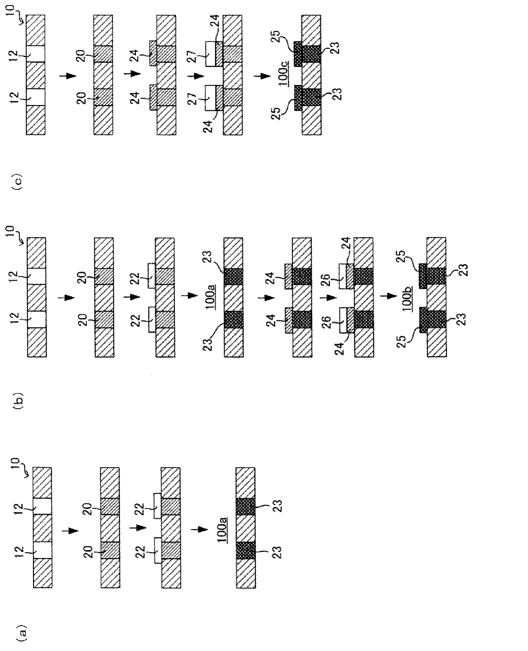
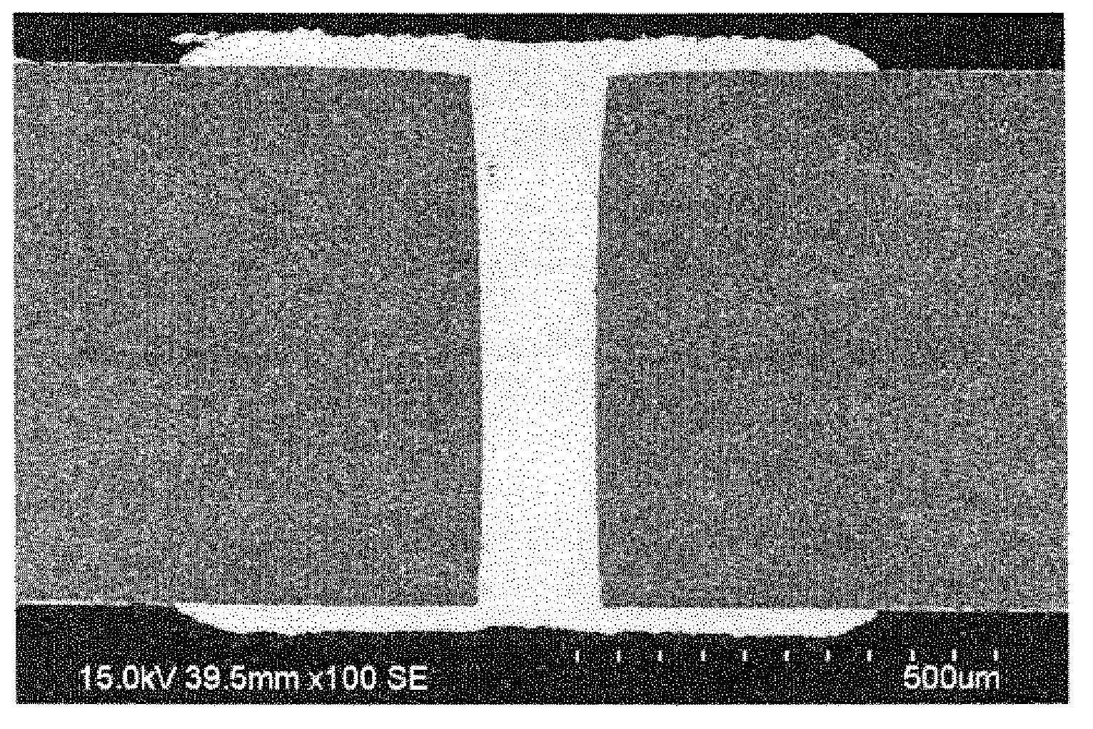
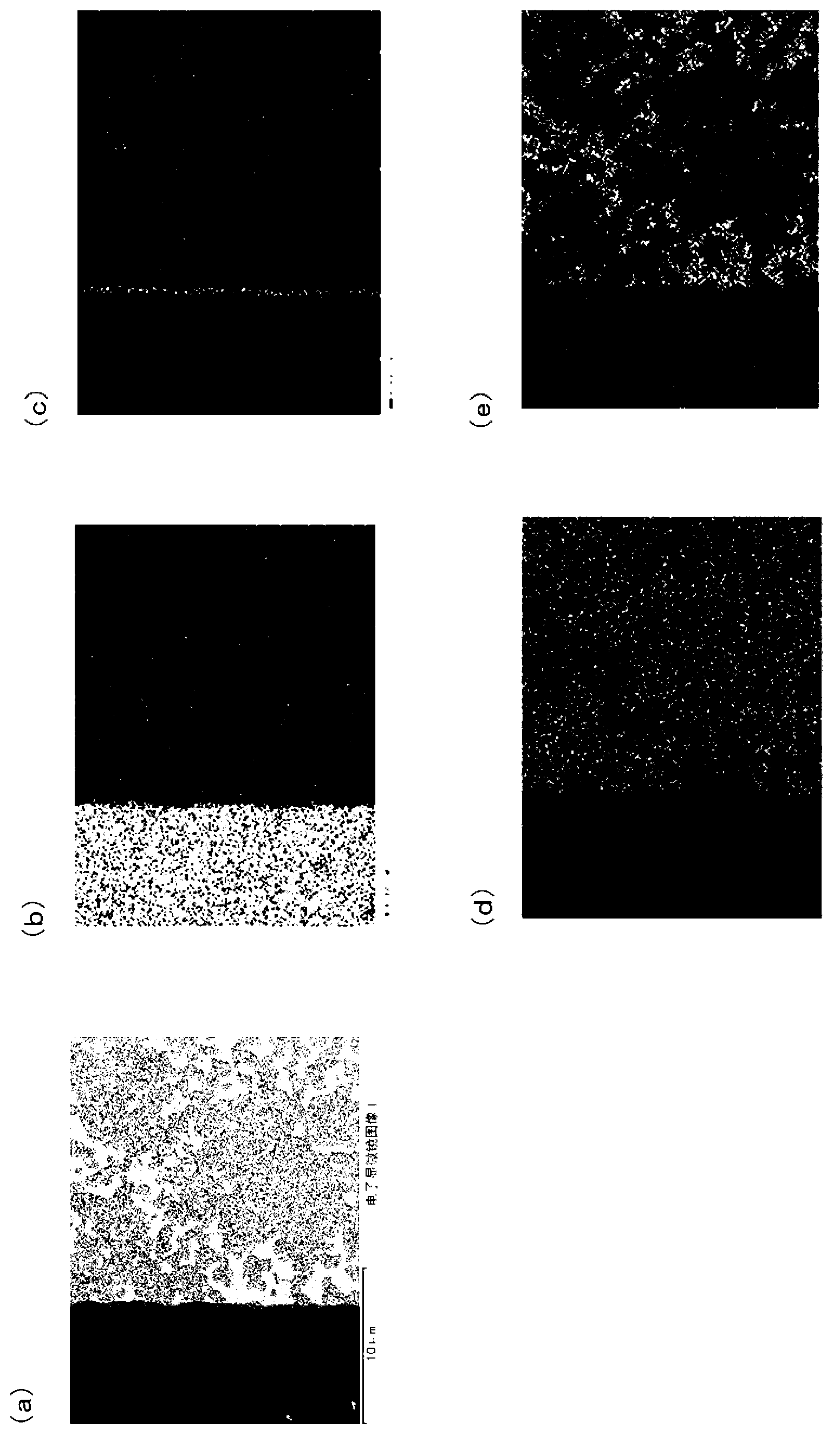
[0173] (Manufacturing of ceramic through-hole substrates)

[0174] (Process (i), process (ii))

[0175] An aluminum ni...

Embodiment 2~5

[0182]

[0183] Except that the raw material composition of the paste was set to the composition shown in Table 1, and the firing conditions were set to the conditions shown in Table 2, it was performed in the same manner as in Example 1 to produce a ceramic through-hole substrate 100a and a metal plate for evaluation. The chemical substrates were analyzed and evaluated as described above. The results are shown in Table 2.

Embodiment 6

[0184]

[0185] (Production of the third metal paste)

[0186] As the metal (B) powder, 12 parts by mass of copper powder with an average particle diameter (D50) of 0.3 μm, 59 parts by mass of copper powder with an average particle diameter (D50) of 2 μm, and 29 parts by mass of an average particle diameter (D50) were used 0.6μm silver powder. A total of 100 parts by mass of metal (B) powder, 5 parts by mass of titanium hydride powder having an average particle diameter (D50) of 5 μm as active metal powder, and polyalkylmethacrylate dissolved in terpineol were mixed using a mortar. The excipients were premixed, and then dispersed by using a 3-roll mixer to prepare a third metal paste.

[0187] (Production of the fourth metal paste)

[0188] As the metal (A) powder, 50 parts by mass of Ag—Cu alloy powder (BAg-8, composition: silver 72 mass %-copper 28 mass %) with an average particle diameter (D50) of 6 μm was used. Among them, 50 parts by mass of copper powder having an a...


PUM

PropertyMeasurementUnit
melting pointaaaaaaaaaa

Abstract

A ceramic via substrate formed by forming conductive via structures in a sintered ceramic substrate, wherein the conductive via structures are formed by tightly filling through-holes with a conductive metal that contains a metal (A) with a melting point of 600 - 1100 DEG C, a metal (B) with a melting point higher than the metal (A), and an active metal, and an active layer is formed at the interface between the conductive via structures and the sintered ceramic substrate. As a result, a ceramic via substrate can be produced by a simple method.

Description

technical field [0001] The present invention relates to ceramic through-hole substrates, metallized ceramic through-hole substrates, and their manufacturing methods. More specifically, it relates to ceramic through-hole substrates and the like used for mounting semiconductor elements such as LEDs, especially for mounting semiconductor elements such as high-output LEDs that dissipate heat. Background technique [0002] A ceramic substrate for mounting a semiconductor element is formed with a metallization pattern on the surface of the ceramic substrate for connection with electrodes of the semiconductor element. In addition, for example, when the ceramic substrate is used as a multilayer substrate or a carrier, the ceramic substrate (hereinafter, a ceramic substrate having conductive via holes and a metallized pattern may be referred to as a "metallized ceramic through-hole substrate". ) to form a conductive through hole for realizing the upper and lower conduction of the su...

Claims


Application Information

Patent Timeline
Patent Type & Authority Applications(China)
IPC IPC(8): H01L23/12H01L23/15H05K1/09H05K1/11H05K3/40
CPCH05K2203/1476H05K3/40H01L23/49827H05K3/4061H01L23/12H05K3/245H05K1/09H05K3/0094H05K1/0306H05K1/092H01L33/62H05K1/11H01L23/15H01L23/14H01L2924/0002H01L2924/00
Inventor 高桥直人山本泰幸
Owner TOKUYAMA CORP
Features
  • Generate Ideas
  • Intellectual Property
  • Life Sciences
  • Materials
  • Tech Scout
  • Unparalleled Data Quality
  • Higher Quality Content
  • 60% Fewer Hallucinations
Learn More