Optical component surface cleaning method based on ion beam polishing

A technology for optical components and surface cleaning, which is applied in the field of ultra-precision processing of optical components, can solve the problems that the KDP crystal surface cleaning method needs to be improved, and achieve the effects of low equipment requirements, reduced roughness value, and guaranteed processing quality

Active Publication Date: 2013-03-27
NAT UNIV OF DEFENSE TECH
View PDF10 Cites 18 Cited by
  • Summary
  • Abstract
  • Description
  • Claims
  • Application Information

AI Technical Summary

Problems solved by technology

The cleaning method of existing KDP cr

Method used


Image

  • Optical component surface cleaning method based on ion beam polishing
  • Optical component surface cleaning method based on ion beam polishing
  • Optical component surface cleaning method based on ion beam polishing

Examples


Embodiment 1

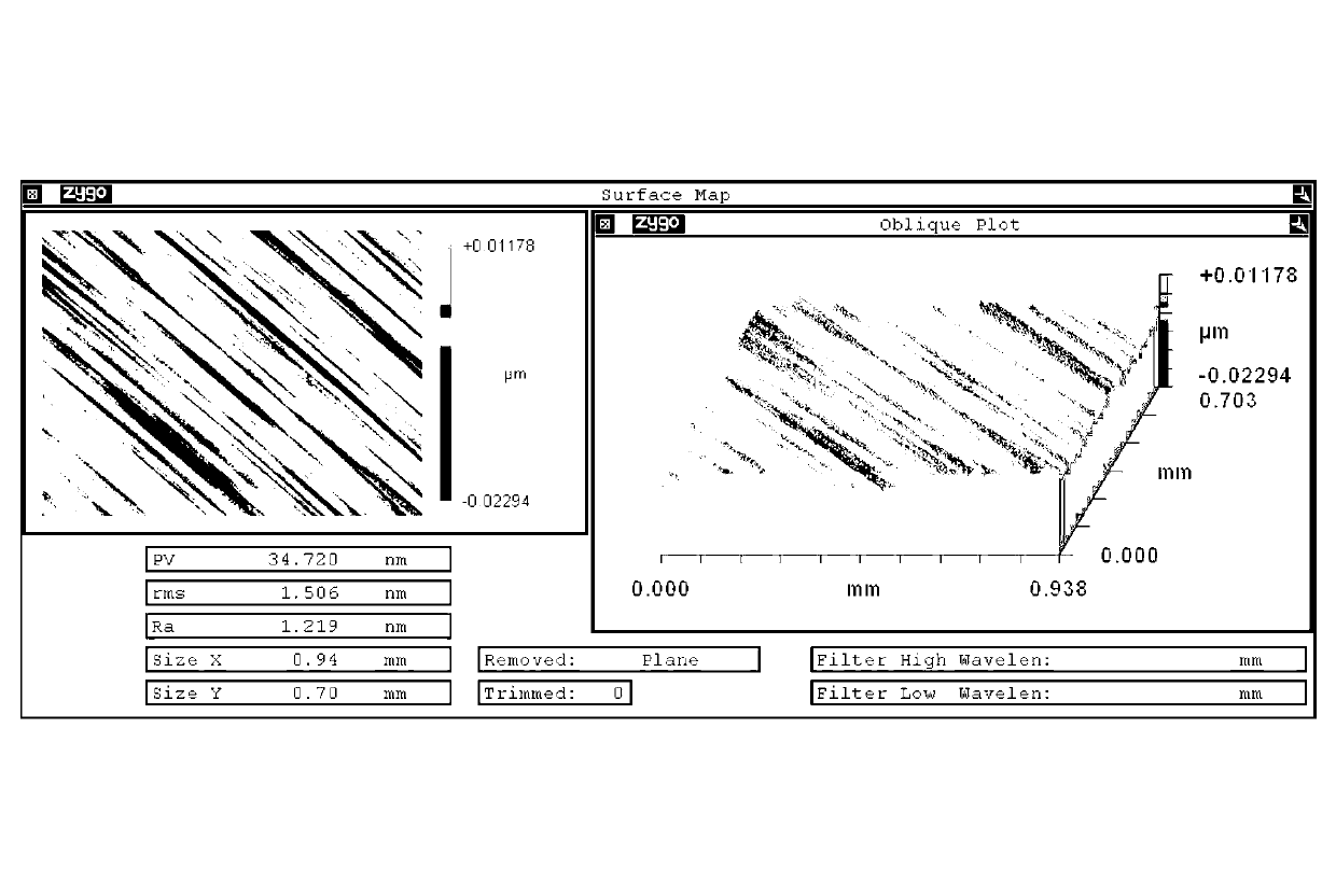
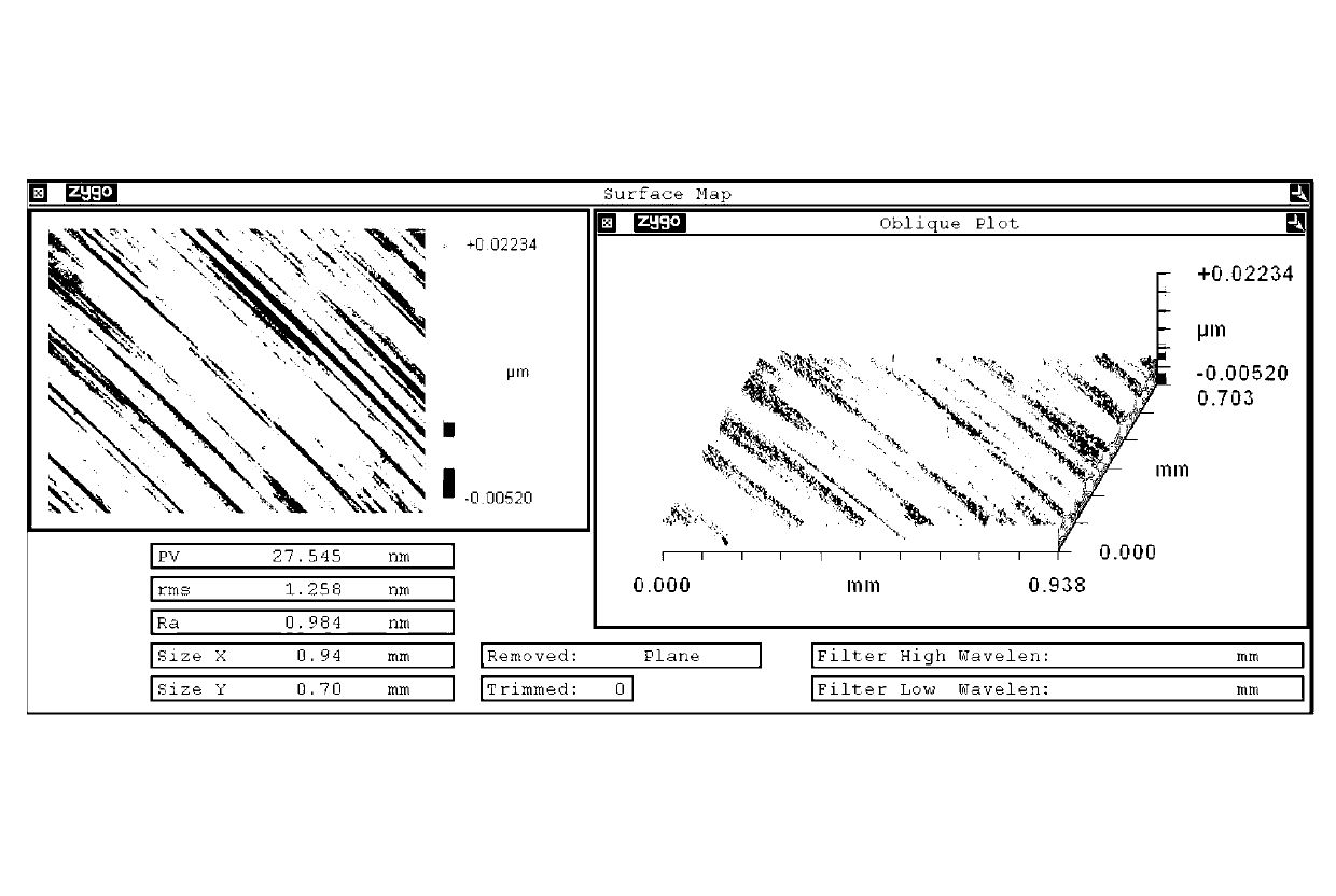
[0023] A method for cleaning the surface of an optical element based on ion beam polishing of the present invention, comprising the following steps: firstly, using single-point diamond turning, the pair of dimensions are 50 × 50 × 10 mm 3 The class II KDP crystal sample 1 and sample 2 were turned, and the main process parameters of single-point diamond turning were controlled as follows: spindle speed 500 r / min, feed rate 2 μm / r, cutting depth 1 μm; The sample 2 of single-point diamond turning is used as the processing object (sample 1 is used as the control), and the surface of the processing object is processed by the ion beam polishing method based on the principle of low-energy ion sputtering. The surface of the component is uniformly scanned, and the main process parameters of ion beam polishing are controlled as follows: incident ion energy 400 eV, ion beam current 30 mA, ion beam incident angle 45° (the image during processing is as follows figure 1 shown); the removal ...

Embodiment 2

[0026] A method for cleaning the surface of an optical element based on ion beam polishing of the present invention, comprising the following steps:

[0027] In order to facilitate the analysis and comparison of the samples by the secondary ion mass spectrometer, three blocks with a size of 8×8×2 mm were selected in this embodiment. 3Type II KDP crystals; among them, sample 3 was subjected to single-point diamond turning; sample 4 was subjected to magnetorheological polishing after single-point diamond turning; sample 5 was subjected to ion beam polishing after single-point diamond turning and magnetorheological polishing (Sample 3 and Sample 4 are used as controls);

[0028] Among them, the process parameters of the single-point diamond turning of each sample are controlled as follows: the spindle speed is 500 r / min, the feed rate is 2 μm / r, and the cutting depth is 1 μm;

[0029] The main process parameters used in the magnetorheological polishing of sample 4 and sample 5 a...


PUM


Abstract

The invention discloses an optical component surface cleaning method based on ion beam polishing. The method comprising the following steps of: machining the surface of a machining object by adopting an ion beam polishing method based on a low-energy ion sputtering principle by taking an optical component subjected to single-point diamond turning or magnetorheological polishing as the machining object; during the machining process, controlling ion beams to uniformly sweep the surface of the optical component; and after the machining is concluded, cleaning the surface of the optical component. The optical component surface cleaning method disclosed by the invention is simple and practicable, low in requirements on equipment, and capable of reducing the surface roughness of the optical surface component and removing the surface impurities of the optical component.

Description

technical field [0001] The invention relates to the technical field of ultra-precision processing of optical elements, in particular to a method for cleaning the surface of optical elements based on low-energy ion sputtering. Background technique [0002] KDP (KH 2 PO 4 ) crystal is a very good nonlinear optical crystal material, which has the characteristics of large nonlinear optical coefficient, wide light transmission band, excellent optical uniformity and high laser damage threshold, etc., and has been widely used It is used in high-tech fields such as laser frequency doubling devices, parametric oscillation, electro-optic modulation, piezoelectric transducers and fast optical switches. Especially in the field of inertial confinement laser nuclear fusion, KDP crystal is the best laser wavelength conversion optical element to improve the efficiency of nuclear fusion reaction. [0003] The inertial confinement fusion ICF laser device requires KDP crystal optical elemen...

Claims


Application Information

Patent Timeline
IPC IPC(8): B24B1/00
Inventor 戴一帆解旭辉袁征周林关朝亮胡皓
Owner NAT UNIV OF DEFENSE TECH
Why Eureka
Try Eureka