Optical proximity correction mask

An optical proximity correction and mask technology, applied in the field of optical lithography, can solve the problems such as the pattern cannot be transferred smoothly, reduce the mask process tolerance, etc., and achieve the effects of reducing light intensity, improving contour, and increasing contrast.

Active Publication Date: 2013-03-27
WINBOND ELECTRONICS CORP
View PDF6 Cites 4 Cited by
  • Summary
  • Abstract
  • Description
  • Claims
  • Application Information

AI Technical Summary

Problems solved by technology

In this way, the pattern of the scattering stripes will become very close to the pattern on the mask (for example, the pattern of the contact hole), thereby reducing the process window for manufacturing the mask, and it is easy to cause cross-linking of adjacent patterns, while The pattern cannot be transferred to the photoresist smoothly

Method used


Image

  • Optical proximity correction mask
  • Optical proximity correction mask
  • Optical proximity correction mask

Examples


Embodiment Construction

[0028] The optical proximity correction mask of the embodiment of the present invention is described below. However, it can be easily understood that the embodiments provided in the present invention are only used to illustrate the making and use of the present invention in a specific way, and are not intended to limit the scope of the present invention.

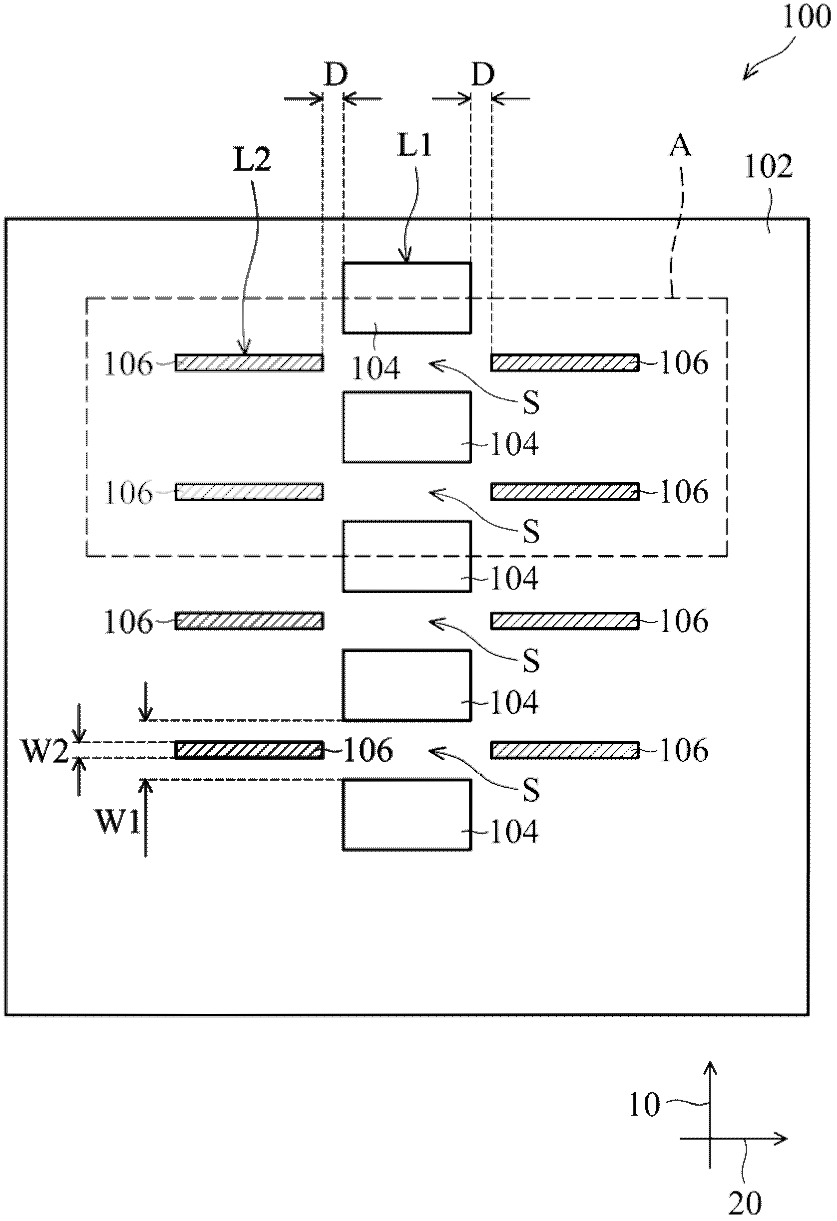
[0029] Please refer to figure 1 , which shows a schematic plan view of the optical proximity correction mask 100 according to an embodiment of the present invention. In this embodiment, the optical proximity correction mask 100 is used to manufacture a semiconductor feature pattern, such as a contact hole, which includes a plurality of opening patterns 104 and a plurality of pairs of scattering bar patterns 106 . These opening patterns 104 are arranged on a substrate 102 (for example, quartz or glass) along a first direction 10, and the substrate 102 is coated with a layer of patterned opaque material (for example, chromium...


PUM


Abstract

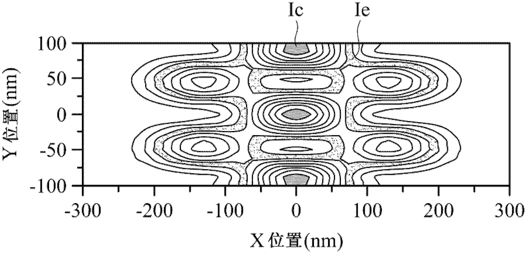
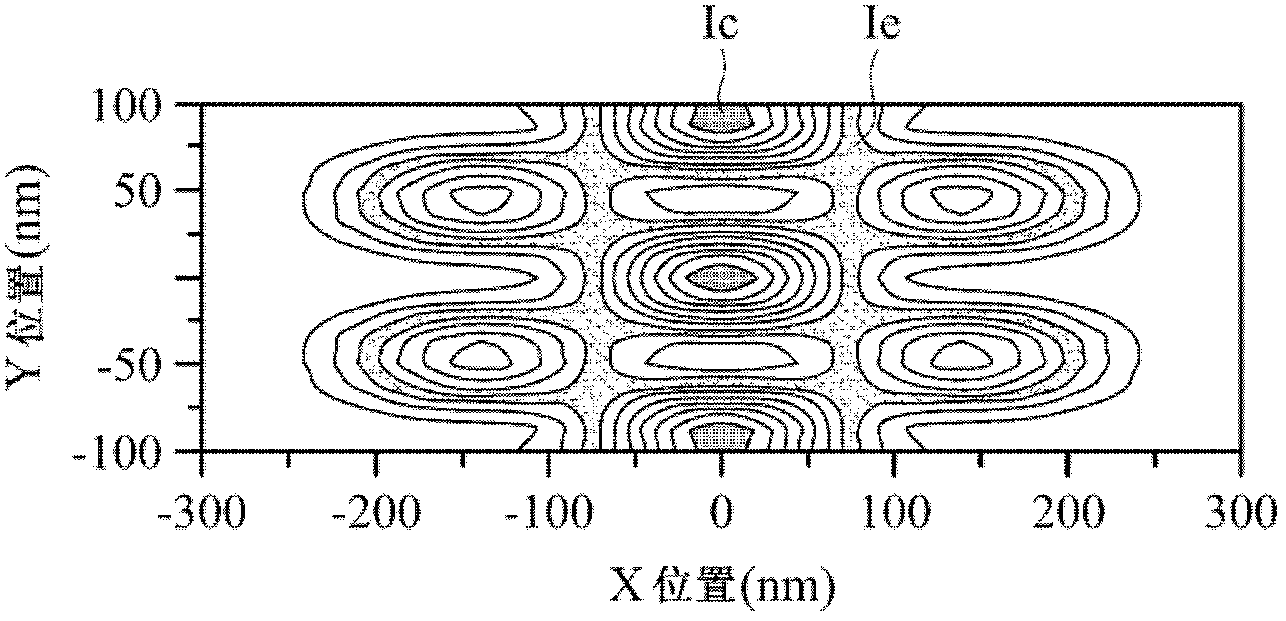
The invention discloses an optical proximity correction mask. The optical proximity correction mask comprises two open patterns and a pair of scattering strip patterns, wherein the open patterns are arrayed on a substrate along a first direction, and there is a fixed distance between the two open patterns; the pair of scattering strip patterns is arranged on the substrate along a second direction vertical to the first direction, and is adjacent to two opposite sides of each of the open patterns; and from a side view, each of the scattering strip patterns does not overlap the open patterns in the first direction or the second direction, and there is a 180DEG phase shift between each of the open patterns and each of the scattering strip patterns. The optical proximity correction mask can reduce the light intensity of the edges of the open patterns, so the contours of the open patterns transferred to a photo-resistor through the mask are improved, and the contrast in a photo-etching process is increased. Additionally, the increase of the contrast in the photo-etching process makes the selective elasticity of a photo-resistive material be increased or makes the technological permissibility of the optical proximity correction mask be further increased.

Description

technical field [0001] The present invention relates to an optical lithography technique, and in particular to an optical proximity correction (OPC) mask for forming a contact hole. Background technique [0002] In semiconductor device manufacturing, patterns corresponding to individual features (eg, contact holes) are usually transferred to photoresists on a wafer through a mask used in a photolithography process. Afterwards, feature patterns are formed on the wafer through an etching process. However, due to light diffraction or other factors, the pattern on the mask cannot be smoothly transferred to the photoresist, which makes it difficult to manufacture the characteristic pattern. Therefore, one of the goals of semiconductor device manufacturing is to enable the original design pattern to be accurately transferred to the photoresist on the wafer through the mask. [0003] At present, many optical proximity correction masks have been developed, so that the original des...

Claims


Application Information

Patent Timeline
Patent Type & Authority Applications(China)
IPC IPC(8): G03F1/36
Inventor 叶癸廷
Owner WINBOND ELECTRONICS CORP
Why Eureka
Try Eureka