Perpendicular lead cold atom chip manufacturing method

A technology of atomic chips and manufacturing methods, applied in semiconductor/solid-state device manufacturing, semiconductor devices, electrical components, etc., can solve problems such as difficult to achieve deep silicon etching, affect the potential energy of annular magnetic traps, reduce chip reliability, etc., and achieve improvement The effect of maximum operating current, reduced chip power consumption, binding capacity and increased reliability

Inactive Publication Date: 2017-06-13
INST OF ELECTRONICS ENG CHINA ACAD OF ENG PHYSICS
View PDF3 Cites 2 Cited by
  • Summary
  • Abstract
  • Description
  • Claims
  • Application Information

AI Technical Summary

Problems solved by technology

Considering the thermal expansion coefficient mismatch between metal and silicon, under high current heating, the large stress at the through hole of the thin silicon wafer will crack the silicon wafer and reduce the reliability of the chip
[0006] 3. After the silicon wafer is thinned to 200um, there is crosstalk between the annular magnetic trap above the silicon wafer and the lead magnetic field below the silicon wafer, which affects the potential energy of the annular magnetic trap
The height of the annular magnetic well on the silicon wafer and the lower leads needs to be greater than 500um to ignore crosstalk, and it is difficult to achieve deep silicon etching with a thickness of more than 500um in the TSV process

Method used


Image

  • Perpendicular lead cold atom chip manufacturing method
  • Perpendicular lead cold atom chip manufacturing method
  • Perpendicular lead cold atom chip manufacturing method

Examples


Embodiment Construction

[0035] In order to further explain the technical means and functions adopted by the present invention to achieve the intended purpose of the invention, the specific implementation of the present invention will be described below in conjunction with the atomic chip design.

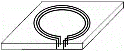
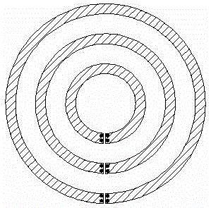
[0036] The circular magnetic trap of the atomic chip is selected to be designed as the first ring radius R1=500um, the second ring radius R2=600um, the third ring radius R3=700um, the ring line width is 90um, and the gap between adjacent ring lines is 10um (design reference physics Journal article ActaPhys.Sin. Vol.65, No.6 (2016) 060302). According to the design, set the vertical lead center distance to 1 / 3 (line width + loop space) = 34um. Gold wire is selected as the vertical lead, the diameter of the gold wire is 12um, and the corresponding maximum fusing current is greater than 5A. The 12um gold wire is the size of conventional bonding gold wire for integrated circuits, which is feasible.

[0037] An...


PUM


Abstract

The invention provides a perpendicular lead cold atom chip manufacturing method. A metal wire embedded in a glass substrate is adopted as magnetic current injection, the technology is characterized in that the metal wire is adopted as an inner core, the glass substrate is manufactured through the technologies of manufacturing of a glass rod, wire drawing, typesetting, glass melt pressing, cutting, fine polishing and the like, and then with the metal wire being an alignment mark on the glass substrate, a metal ring magnetic well is manufactured to form an atom chip through a semiconductor micro-nano technology. The perpendicular lead cold atom chip manufacturing method has the advantages that by adopting the glass substrate embedded with the metal wire to manufacture the atom chip, the specific resistance of the metal wire is far smaller than plated metal, and the phenomenon that heating under big current fuses a lead is avoided; the glass substrate can reach a nanometer thickness, and can effectively lower magnetic field interference of circuit loops at the front side and the back side of the substrate.

Description

technical field [0001] The invention belongs to the technical field of magneto-optical trap cold atom trapping and the application field of atomic chip gyroscopes, and in particular relates to a method for manufacturing an atomic chip with a vertical lead structure. Background technique [0002] Atomic gyroscopes can be realized based on matter wave interference, and ring magnetic guidance technology is the key to the miniaturization of atomic interference gyroscopes. The annular magnetic guiding structure can be fabricated on the chip using micro-nano processing technology, which has the advantages of small size and strong magnetic trap binding ability. The existing atomic chip annular magnetic guidance structure such as figure 1 As shown, there are shortcomings such as large gaps in the current leads, failure to form a closed annular magnetic trap, or weak binding of the annular magnetic trap. In 2016, an article proposed a vertical wire atomic chip structure [Acta Phys....

Claims


Application Information

Patent Timeline
Patent Type & Authority Applications(China)
IPC IPC(8): H01L21/56H01L21/60
CPCH01L24/43H01L21/56
Inventor 王旺平李沫陈飞良周晟姜伟赵杰张健
Owner INST OF ELECTRONICS ENG CHINA ACAD OF ENG PHYSICS
Why Eureka
Try Eureka