Photoelectric monolithic integration system based on multi-material system

A monolithic integration, multi-material technology, applied in the direction of light guide, optics, optical components, etc., can solve the problems of high monolithic integration cost of indium phosphide, large loss of silicon-based modulator, difficulty in large-scale integration, etc., and achieve excellent electro-optic Effects of Performance, Improved Performance, Low Polarization Sensitivity

Active Publication Date: 2020-07-31
SHANGHAI JIAO TONG UNIV
View PDF4 Cites 2 Cited by
  • Summary
  • Abstract
  • Description
  • Claims
  • Application Information

AI Technical Summary

Problems solved by technology

However, the shortcomings of these two material platforms are: silicon-based monolithic integration is difficult to integrate active devices such as light sources, silicon-based modulators have large losses and high half-wave voltages; indium phosphide monolithic integration costs are high, and it is difficult to achieve large-scale integrated

Method used


Image

  • Photoelectric monolithic integration system based on multi-material system
  • Photoelectric monolithic integration system based on multi-material system
  • Photoelectric monolithic integration system based on multi-material system

Examples


Embodiment Construction

[0046] The following is a detailed description of the embodiments of the present invention: this embodiment is implemented on the premise of the technical solution of the present invention, and provides detailed implementation methods and specific operation processes. It should be noted that those skilled in the art can make several modifications and improvements without departing from the concept of the present invention, and these all belong to the protection scope of the present invention.

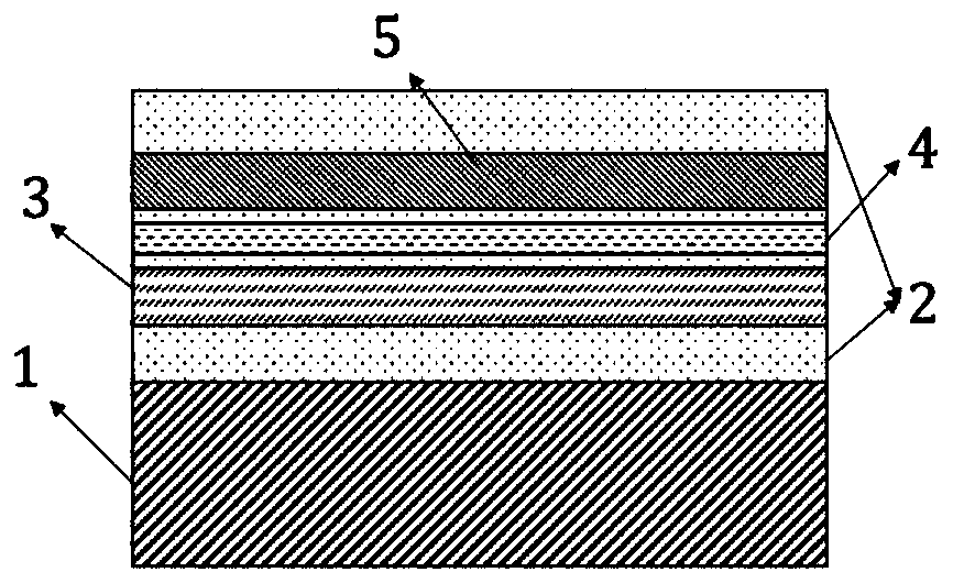
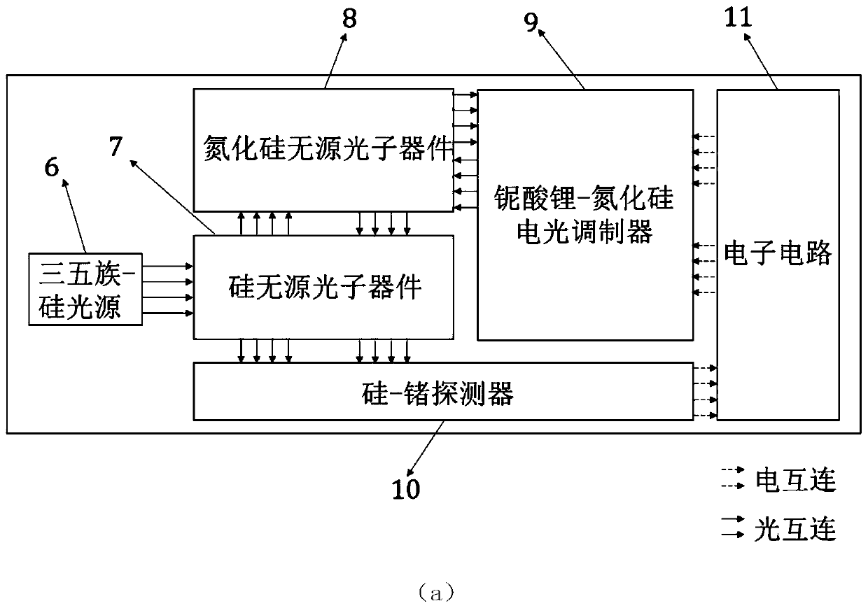
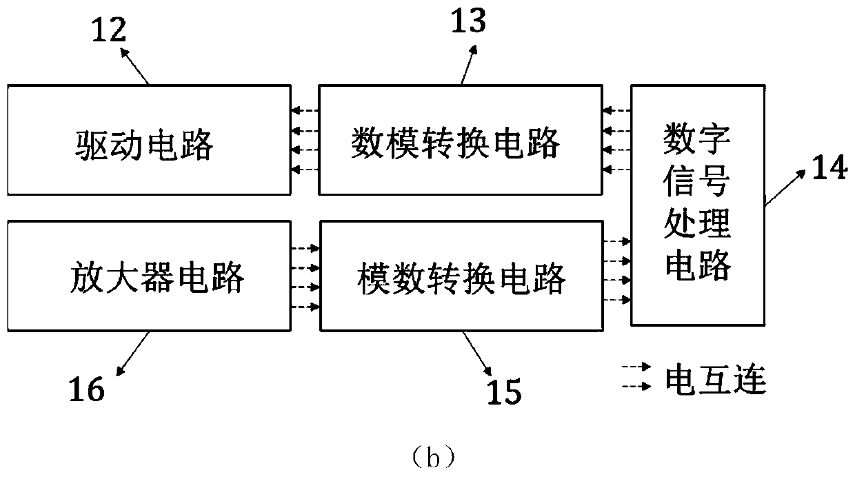
[0047] An embodiment of the present invention provides a photoelectric monolithic integrated system based on a multi-material system, including: a silicon substrate layer, a lithium niobate thin film layer, a silicon nitride thin film layer and a silicon thin film layer, an indium phosphide thin film layer, and a germanium thin film layer . Between the silicon substrate layer and the lithium niobate thin film layer, between the lithium niobate thin film layer and the silicon nitride thi...


PUM


Abstract

The invention provides a photoelectric monolithic integration system based on a multi-material system. According to the system, an indium phosphide-silicon laser, a silicon passive photonic device, asilicon nitride passive photonic device, a silicon nitride-lithium niobate electro-optical modulator, a germanium-silicon detector and an electronic circuit are integrated on the same substrate, so that the size of a photoelectric system is reduced, the electrical and optical interconnection distance is reduced, and the adverse effect of parasitic parameters on the integrated system is greatly reduced. The packaging between the optical path module and the circuit module is avoided, and the packaging cost is reduced. The advantages of excellent electro-optical performance of the lithium niobatematerial, low loss, low polarization sensitivity and high process tolerance of the silicon nitride material and high refractive index of the silicon material are exerted, and a monolithic photoelectric integrated system with excellent performance is realized.

Description

technical field [0001] The invention relates to the technical field of monolithic photoelectric heterogeneous integration, in particular to a photoelectric monolithic integration system based on a multi-material system. Background technique [0002] The optoelectronic system combines the transmission advantages of light and the processing advantages of electricity, and can realize high-speed signal transmission and processing. The integration of optoelectronic systems can be realized by hybrid integration technology or heterogeneous integration technology. Hybrid integration is the integration of optoelectronic devices and electronic devices through packaging technology. Compared with hybrid integration, optoelectronic monolithic integration technology greatly reduces system volume, power consumption, parasitic parameters and packaging costs by integrating optoelectronic devices, electronics and electronic circuits on the same substrate, and finally achieves high-speed, hig...

Claims


Application Information

Patent Timeline
Patent Type & Authority Applications(China)
IPC IPC(8): G02F1/035G02F1/03G02B6/12G02B6/42
CPCG02B6/12G02B6/42G02B2006/12035G02B2006/1204G02B2006/12061G02B2006/12142G02B2006/12147G02B2006/12159G02B2006/12164G02F1/0327G02F1/035
Inventor 邹卫文王静徐绍夫
Owner SHANGHAI JIAO TONG UNIV
Why Eureka
Try Eureka