A patterned sapphire substrate and a preparation method thereof

A patterned sapphire and sapphire technology, which is applied to electrical components, circuits, semiconductor devices, etc., can solve the problems of difficult etching and high hardness, and achieve the effects of improving luminous efficiency, high process tolerance, and reducing production costs

Active Publication Date: 2019-01-08
孙逊运
View PDF9 Cites 1 Cited by
  • Summary
  • Abstract
  • Description
  • Claims
  • Application Information

AI Technical Summary

Problems solved by technology

[0005] The first object of the present invention is to provide a patterned sapphire substrate to solve the technical problem in the prior art that the sapphire

Method used


Image

  • A patterned sapphire substrate and a preparation method thereof
  • A patterned sapphire substrate and a preparation method thereof
  • A patterned sapphire substrate and a preparation method thereof

Examples


Example Embodiment

[0051] Example 1

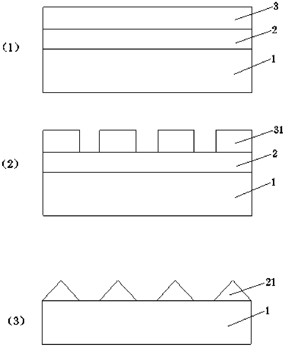
[0052] see image 3 , which is a schematic diagram of the process structure of preparing a patterned sapphire substrate in this embodiment, wherein (1) is a schematic cross-sectional structure of coating to form a silicon-containing organic coating and a photoresist; (2) is a photoresist layer formed A schematic cross-sectional structure diagram of the mask pattern; (3) is a cross-sectional structure schematic diagram of transferring the pattern to the silicon-containing organic coating after the etching is completed.

[0053] The preparation method of the patterned sapphire substrate described in this embodiment includes the following steps:

[0054] (a) coating the surface of the sapphire flat sheet 1 to form a silicon-containing organic coating 2; specifically,

[0055] (a1) the surface of the sapphire flat sheet 1 is subjected to purification pretreatment: the sapphire flat sheet 1 is placed in trichloroethane, ultrasonically cleaned for 10min, then pl...

Example Embodiment

[0064] Example 2

[0065] see Figure 4 , which is a schematic structural diagram of the process of preparing a patterned sapphire substrate in this embodiment, wherein (1) is a schematic cross-sectional structure of coating to form a silicon-containing organic coating, an etching-resistant coating and a photoresist; (2) is Schematic diagram of the cross-sectional structure of forming the photoresist layer into a mask pattern; (3) is a schematic diagram of the cross-sectional structure of transferring the pattern to the etch-resistant coating; (4) is the cross-section of the pattern transferred to the silicon-containing organic coating after the etching is completed Schematic.

[0066] The preparation method of the patterned sapphire substrate described in this embodiment includes the following steps:

[0067] (a) coating the surface of the sapphire flat sheet 1 to form a silicon-containing organic coating 2; specifically,

[0068] (a1) the surface of the sapphire flat shee...


PUM

PropertyMeasurementUnit
Thicknessaaaaaaaaaa
Thicknessaaaaaaaaaa
Thicknessaaaaaaaaaa

Abstract

The invention relates to the technical field of semiconductor manufacturing, in particular to a patterned sapphire substrate and a preparation method thereof. The patterned sapphire substrate comprises a sapphire flat sheet and a patterned silicon-containing organic coating formed on the surface thereof. A manufacture method comprises that follow steps of: (a) coating a silicon-containing organiccoating on the surface of a sapphire flat sheet; (b) coat a photoresist on that surface of the silicon-containing organic coating to form a photoresist layer, and photolithographically forming a maskpattern; (c) etching the silicon-containing organic coating under the protection of the photoresist layer, transferring the pattern to the silicon-containing organic coating, and removing the photoresist to obtain the patterned sapphire substrate. The invention replaces the traditional patterned sapphire substrate with a patterned silicon-containing organic coating, wherein the refractive index ofthe silicon-containing organic coating is lower than that of the sapphire, the scattering effect of the substrate on light can be effectively increased, and the luminous efficiency of the LED can beimproved; Moreover, its hardness is lower than that of sapphire, which increases the tolerance of photolithography and etching process and reduces the production cost.

Description

technical field [0001] The invention relates to the technical field of semiconductor manufacturing, in particular to a patterned sapphire substrate and a preparation method thereof. Background technique [0002] At present, the most ideal and most widely used material for LED light-emitting diodes is gallium nitride (GaN), but it is very difficult to prepare gallium nitride single crystal materials, and there is no effective method. Epitaxial growth of gallium nitride materials is performed on substrates with similar lattice structures such as sapphire and silicon carbide. Sapphire has the advantages of good mechanical properties and chemical stability, no absorption of visible light, and relatively mature manufacturing technology. It is currently the most ideal substrate material for LEDs. Compared with the common sapphire flat wafer substrate, the patterned sapphire substrate (PSS) with specific regular microstructure pattern is fabricated on its surface, and its surface ...

Claims


Application Information

Patent Timeline
IPC IPC(8): H01L33/20H01L33/22H01L33/16
CPCH01L33/16H01L33/20H01L33/22
Inventor 孙逊运
Owner 孙逊运
Why Eureka
Try Eureka