Composite semiconductor layer

A compound semiconductor, covering layer technology, applied in the direction of semiconductor devices, semiconductor/solid-state device components, electric solid-state devices, etc., to achieve the effect of stable and reliable magnetic moment

Active Publication Date: 2013-03-27
INST OF PHYSICS - CHINESE ACAD OF SCI
View PDF5 Cites 3 Cited by
  • Summary
  • Abstract
  • Description
  • Claims
  • Application Information

AI Technical Summary

Problems solved by technology

Under the current technical conditions, devices made of semiconductor materials alone cannot meet the existing requirements

Method used


Image

  • Composite semiconductor layer
  • Composite semiconductor layer
  • Composite semiconductor layer

Examples


Embodiment 1

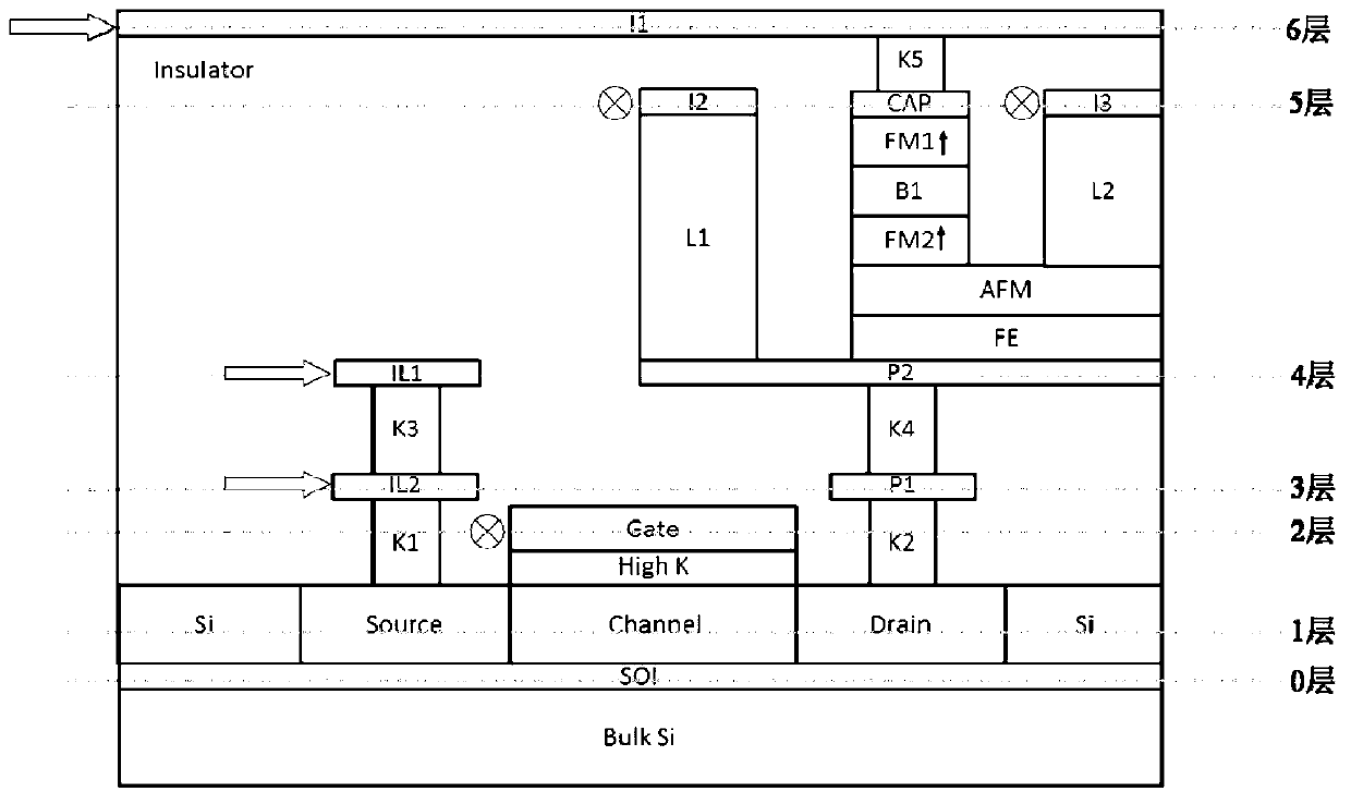
[0067] A kind of magnetic random storage unit based on electric current drive that the compound semiconductor layer of the present invention can provide, the circuit symbol is as Figure 3B As shown, its core structure is AFM / FM2 / B1 / FM1, including:

[0068] Input / output signal lines I1, I3;

[0069] Through hole L2;

[0070] Antiferromagnetic layer AFM;

[0071] The lower magnetic layer FM2;

[0072] Tunnel insulation barrier layer B1;

[0073] upper magnetic layer FM1;

[0074] Top cover layer CAP;

[0075] The composition material of the input / output signal line and the through hole is a metal with good conductivity commonly used in semiconductor technology, such as Cu.

[0076] The composition material of the antiferromagnetic layer (AFM) includes Ir, Fe, Rh, Pt or alloy materials of Pd and Mn, or antiferromagnetic materials such as CoO, NiO, PtCr, etc.

[0077] The composition materials of the two magnetic layers (the lower magnetic layer FM2 and the upper magnetic ...

Embodiment 2

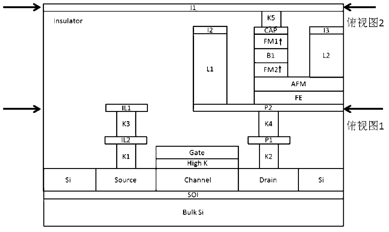
[0085] A highly sensitive magnetic sensor unit based on the compound semiconductor layer of the present invention, the circuit symbol is as Figure 3C shown. Its core structure is FE / AFM / FM2 / B1 / FM1, including:

[0086] Input / output signal lines I1, I3;

[0087] Control signal line I2;

[0088] Through holes L1, L2;

[0089] metal platform P2;

[0090] Ferroelectric layer FE;

[0091] Antiferromagnetic layer AFM;

[0092] The lower magnetic layer FM2;

[0093] Tunnel insulation barrier layer B1;

[0094] upper magnetic layer FM1;

[0095] Top cover layer CAP;

[0096] The input / output signal lines, the control signal lines, the through holes and the metal platform are made of a metal with good conductivity commonly used in semiconductor technology, such as Cu.

[0097] The composition material of the ferroelectric layer (FE) includes BiFeO3 (BFO), BaTiO3 (BTO), SrTiO3 (STO), Pb (Mg1 / 3Nb2 / 3) O3-PbTiO3 (PMN-PT), PbTiO3 (PTO), BiMnO3, etc.;

[0098] The composition mat...

Embodiment 3

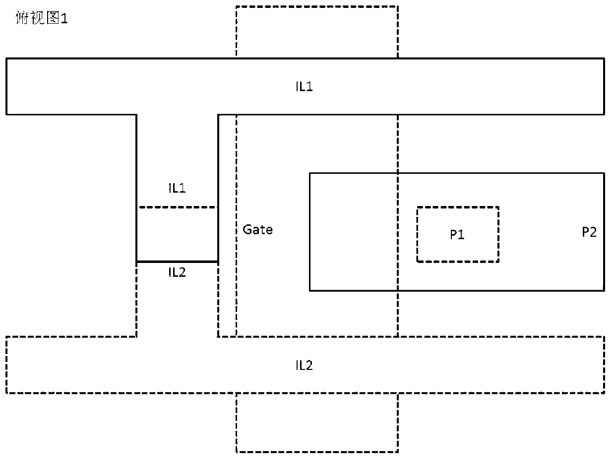
[0107] Based on the compound semiconductor layer of the present invention, a logic judgment unit can be provided, and the circuit symbol is as follows: Figure 3D shown. Its core structure is AFM / FM2 / B1 / FM1, including:

[0108] Control / output signal lines I1, I3;

[0109] Input signal lines IL1, IL2;

[0110] Through hole L2;

[0111] Vias K1, K3, K5;

[0112] Field effect tube FET;

[0113] Antiferromagnetic layer AFM;

[0114] The lower magnetic layer FM2;

[0115] Tunnel insulation barrier layer B1;

[0116] upper magnetic layer FM1;

[0117] Top cover layer CAP;

[0118] The control / output signal line, the input signal line, the through hole or the constituent material of the via hole is a metal with good conductivity commonly used in semiconductor technology, such as Cu.

[0119] The composition material of the antiferromagnetic layer (AFM) includes Ir, Fe, Rh, Pt or alloy materials of Pd and Mn, or antiferromagnetic materials such as CoO, NiO, PtCr, etc.

[01...


PUM


Abstract

The invention provides a composite semiconductor layer which comprises a silicon-on-insulator (SOI) substrate and a filed effect transistor. The SOI substrate is deposited on a bulk silicon material, and a silicon film is deposited on the SOI substrate. The field effect transistor is arranged on the silicon film, a source electrode of the field effect transistor is connected onto a second auxiliary input/output signal line through a first via hole, the second auxiliary input/output signal line is connected onto a first auxiliary input/output signal line through a third via hole, a drain electrode is connected onto a first metal electrode through a second via hole, the first metal electrode is connected onto a second metal electrode through a fourth via hole, one end of the second metal electrode is connected onto a second input/output signal line through a first through hole, and a ferroelectric layer, an antiferromagnetic layer, a lower ferromagnetic layer, a tunnel insulating barrier layer, an upper ferromagnetic layer and a top cover layer are sequentially deposited at the other end of the second metal electrode. The antiferromagnetic layer is connected onto a third input/output signal line through a second through hole, and the top cover layer is connected onto the first input/output signal line through a fifth via hole.

Description

technical field [0001] The invention relates to the field of semiconductors, in particular to a compound semiconductor layer in a planar integrated system for micro intelligent robots. Background technique [0002] As we all know, micro intelligent robots have been widely used in various fields, such as information collection, automatic control, medical rescue and so on. Generally speaking, the electronic control system of the mechanical part of the micro robot can be divided into: information collection module (sensor unit), information processing module (logic operation unit), information storage module (storage medium unit), information communication module (microwave transmission unit), task management module, and system boot module. The task management module and the system guidance module can be constructed by a logic operation unit and a storage medium unit. [0003] At present, micro-intelligent robots are mainly facing two major problems: first, the reliability of...

Claims


Application Information

Patent Timeline
Patent Type & Authority Applications(China)
IPC IPC(8): H01L23/522H01L23/64
Inventor 郭鹏刘东屏韩秀峰
Owner INST OF PHYSICS - CHINESE ACAD OF SCI
Why Eureka
Try Eureka