Complementary metal oxide semiconductor (CMOS) circuit structure and manufacture method and display device thereof

A circuit structure and semiconductor technology, applied in circuits, electrical components, electrical solid devices, etc., can solve the problems of complex production process, high production cost, increase production cost, etc., to simplify production process, reduce production cost, and prolong service life. Effect

Active Publication Date: 2013-03-27
BOE TECH GRP CO LTD
View PDF5 Cites 73 Cited by
  • Summary
  • Abstract
  • Description
  • Claims
  • Application Information

AI Technical Summary

Problems solved by technology

[0016] In the above-mentioned process of preparing CMOS circuits using the LTPS process, it is necessary to use at least 10 or more photoresist masks and at least 4 or more doping processes (P-type ion doping, N-type ion doping, LDD doping, etc.) and Ch doping), the production process is complex, the production cost is high, and, in step 1, the entire layer of a-Si material needs to be laser crystallized to obtain polysilicon material, and the long-time laser crystallization process will increase the product’s Production cost, and will reduce the service life of the laser tube, but also increase the production cost

Method used


Image

  • Complementary metal oxide semiconductor (CMOS) circuit structure and manufacture method and display device thereof
  • Complementary metal oxide semiconductor (CMOS) circuit structure and manufacture method and display device thereof
  • Complementary metal oxide semiconductor (CMOS) circuit structure and manufacture method and display device thereof

Examples


Embodiment Construction

[0035] The specific implementation manners of the CMOS circuit structure provided by the embodiments of the present invention, its manufacturing method and the display device will be described in detail below with reference to the accompanying drawings.

[0036] The shape and size of each region in the drawings do not reflect the real scale of the CMOS circuit structure, but are only intended to schematically illustrate the content of the present invention.

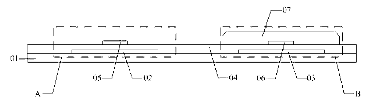
[0037] A kind of CMOS circuit structure that the embodiment of the present invention provides, such as figure 2 As shown, there is a PMOS region C and an NMOS region D, including: a PMOS semiconductor layer 22, a gate insulating layer 23, a PMOS gate 24 and an NMOS gate 25, and a first interlayer dielectric layer 26 located on the base substrate 21 in sequence. , NMOS semiconductor layer 27, second interlayer dielectric layer 28, PMOS source and drain electrodes 29 and NMOS source and drain electrodes 30, wherein,

[00...


PUM


Abstract

The invention discloses a complementary metal oxide semiconductor (CMOS) circuit structure and a manufacture method and a display device thereof. A P-channel metal oxide semiconductor (PMOS) area in the CMOS circuit structure is of a low temperature poly silicon (LTPS) thin film transistor (TFT) structure, namely a P type mingled polycrystalline silicon material is utilized to prepare a PMOS layer. An N-channel metal oxide semiconductor (NMOS) area is of an Oxide TFT structure, namely an oxide material is utilized to prepare an NMOS layer. The oxide material is utilized at the NMOS area to replace the existing polycrystalline silicon material to prepare the NMOS layer, three mingled processes of the NMOS area in the LTPS process are saved, manufacture flow of the CMOS circuit structure is simplified, and production cost is reduced. Further, the oxide material is adopted to manufacture the NMOS layer of the NMOS area, crystallization is only needed to be conducted on the PMOS layer in the PMOS area, service life of a laser tube is prolonged, and production cost is reduced.

Description

technical field [0001] The invention relates to the technical field of circuit manufacturing, in particular to a CMOS circuit structure, a preparation method thereof and a display device. Background technique [0002] Complementary Metal Oxide Semiconductor (CMOS, Complementary Metal Oxide Semiconductor) is composed of P-channel Metal Oxide Semiconductor (PMOS, Positive channel MetalOxide Semiconductor) and N-channel Metal Oxide Semiconductor (NMOS, Negativechannel-Metal-Oxide-Semiconductor). constitute. [0003] At present, low temperature polysilicon (LTPS, Low Temperature Poly-silicon) technology is generally used to prepare the semiconductor layers of the PMOS region and the NMOS region in the CMOS circuit respectively. The preparation process is relatively complicated, and the specific process steps are as follows: [0004] Step 1: On the base substrate 01, use a patterning process to form the pattern of the PMOS semiconductor layer 02 located in the PMOS area A, and t...

Claims


Application Information

Patent Timeline
Patent Type & Authority Applications(China)
IPC IPC(8): H01L27/092H01L21/77H01L21/8258
CPCH01L27/1251H01L29/7869H01L27/1225
Inventor 任章淳
Owner BOE TECH GRP CO LTD
Why Eureka
Try Eureka