Light emitting diode chip having wavelength conversion layer and manufacturing method thereof, and package including same and manufacturing method thereof

A technology of wavelength conversion layer and light-emitting diode, which is applied in the field of package and its manufacture, light-emitting diode chip with wavelength conversion layer and its manufacture, to achieve the effect of reducing heat dissipation path and easy bonding of wires

Active Publication Date: 2013-03-27
SEOUL SEMICONDUCTOR
View PDF7 Cites 29 Cited by
  • Summary
  • Abstract
  • Description
  • Claims
  • Application Information

AI Technical Summary

Problems solved by technology

[0006] However, since the wavelength conversion sheet is pasted on the upper surface of the LED, it is limited to the case

Method used


Image

  • Light emitting diode chip having wavelength conversion layer and manufacturing method thereof, and package including same and manufacturing method thereof
  • Light emitting diode chip having wavelength conversion layer and manufacturing method thereof, and package including same and manufacturing method thereof
  • Light emitting diode chip having wavelength conversion layer and manufacturing method thereof, and package including same and manufacturing method thereof

Examples


Embodiment Construction

[0094] Hereinafter, various embodiments of the present invention will be described in detail with reference to the drawings. The embodiments described below are provided as examples in order to fully convey the idea of ​​the present invention to those skilled in the art. Therefore, the present invention is not limited to the Examples described below, and may be embodied in other forms. In addition, in the drawings, the width, length, thickness, etc. of the constituent elements may be exaggerated for convenience of description. Throughout the specification, the same reference numerals denote the same constituent elements.

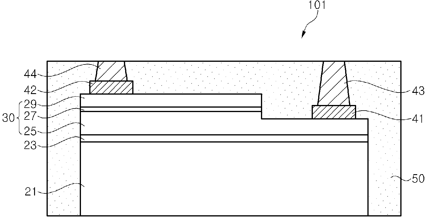
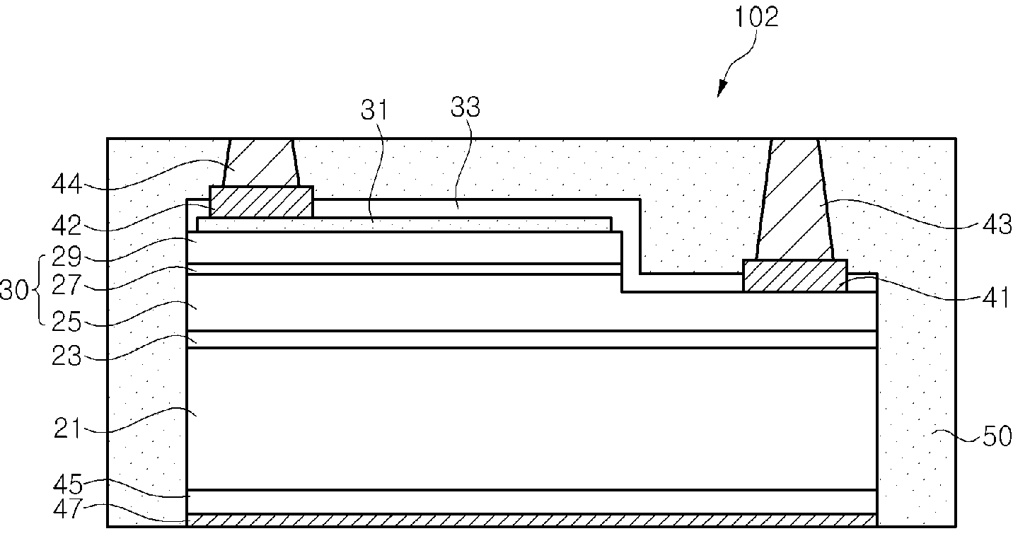
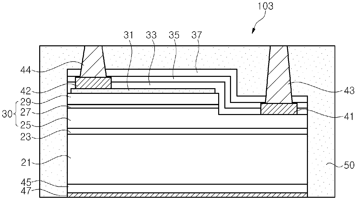
[0095] figure 1 A cross-sectional view of the LED chip 101 provided for illustrating an embodiment of the present invention.

[0096] The light emitting diode chip 101 includes: a substrate 21; a GaN-based semiconductor stacked structure 30 including a first conductivity type semiconductor layer 25, an active layer 27, and a second conductivity type semic...


PUM


Abstract

Disclosed are a light emitting diode chip having a wavelength conversion layer, a method for manufacturing the same, and a package having the same. According to one aspect, the light emitting diode chip comprises: a substrate; a semiconductor stacked structure, which is located on an upper surface of the substrate and a gallium nitride-based compound semiconductor stacked structure including a first conductive semiconductor layer, an active layer, and a second conductive semiconductor layer; an electrode which is electrically connected to the semiconductor stacked structure; an additional electrode which is formed on said electrode; and a wavelength conversion layer which covers the upper part of the semiconductor stacked structure. Further, said additional electrode passes through the wavelength conversion layer. Thus, the invention is capable of performing wavelength conversion of light, and providing a light emitting diode chip which can easily bond a wire.

Description

technical field [0001] The invention relates to a light-emitting diode chip and its manufacturing method, as well as its package and its manufacturing method, in particular to a light-emitting diode chip with a wavelength conversion layer and its manufacturing method, as well as its package and its manufacturing method. Background technique [0002] Since the current light-emitting diodes have the advantages of being able to realize thinness, lightness and miniaturization, save energy and maintain life for a long time, they are being used as backlight sources for various display devices including mobile phones, and due to the advantages of mounting light-emitting diodes A light-emitting element (ie, a light-emitting diode package) can realize white light with high color rendering, and thus is expected to be applied to general lighting in place of white light sources such as fluorescent lamps. [0003] In addition, there are various methods of realizing white light using ligh...

Claims


Application Information

Patent Timeline
IPC IPC(8): H01L33/50H01L33/36
CPCH01L2224/92247H01L2224/8592H01L2224/49107H01L2224/48091H01L2224/06102H01L2224/1403
Inventor 郑井和金枋显
Owner SEOUL SEMICONDUCTOR
Why Eureka
Try Eureka