


Quick Research
Generate reliable direction feasibility study reports for your R&D in just a few steps.

Technical Q&A
Discover and master advanced knowledge NOW. Basics, ideas, possibilities, all at once.

Find Solutions
As an expert in R&D theories, this can generate solutions to your technical problems instantly.

Evaluate Feasibility
Analyze your overall solution with one click, know your potential R&D risks in advance.

Monitor Landscape
Get weekly tech updates, stay abreast of the latest tech innovations and key insights.
Preparation method of NPC (nano porous copper) thin films
A nanoporous copper and thin film technology, applied in the field of nanoporous metals and its preparation, can solve the problems of not being suitable for integration, etc., and achieve the effects of good uniformity, improved sputtering efficiency, and large area
- Summary
- Abstract
- Description
- Claims
- Application Information
AI Technical Summary
Problems solved by technology
Method used
Image

Examples
Embodiment 1
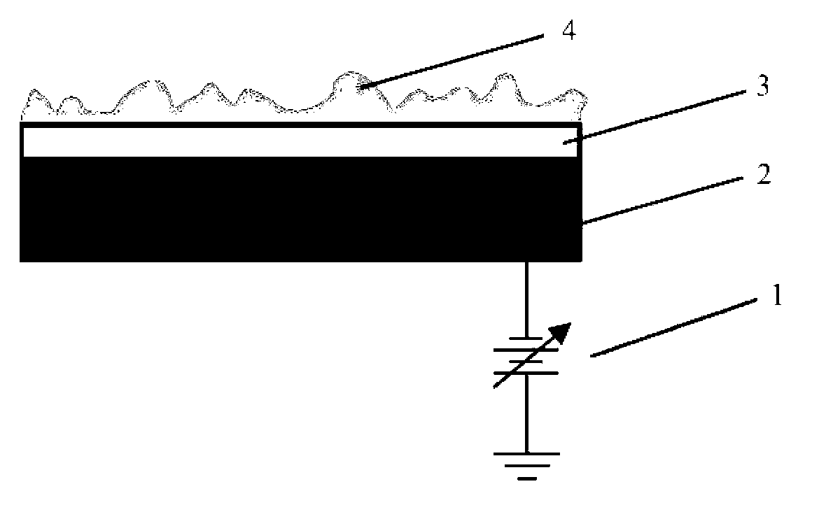
[0022] 1) Using the JGP500A BMS coating system, first fix the clean glass slide substrate on the sample tray, then install the copper target with a purity of 99.99% on the RF source, and adjust the distance between the substrate and the copper target is 15cm;
[0023] 2) Close the chamber door and evacuate to 5.0×10 -4 Pa, then pass high-purity Ar gas with a flow rate of 15sccm and a purity of 99.999%, and keep the chamber pressure at 0.1pa;
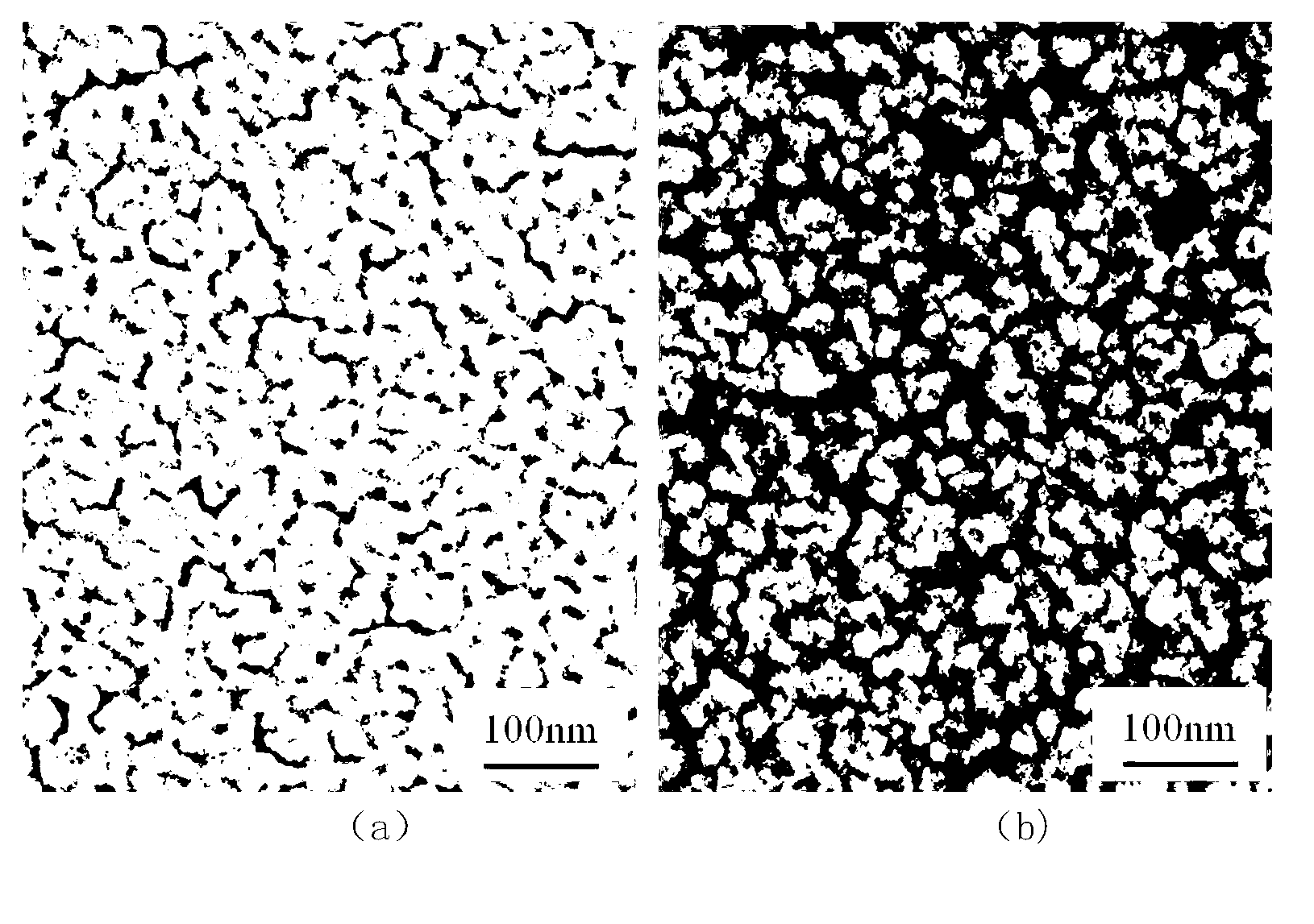
[0024] 3) Pre-sputter a 30nm-thick copper film on the glass slide with RF 100W power at room temperature and no applied bias voltage (see figure 2 (a)), as the direct substrate of NPC thin films;
[0025] 4) Under the condition of room temperature and applied bias voltage of DC–100V, the power of RF 100W was used for further sputtering deposition of 120 nm to obtain a porous triangular prism-like structure NPC thin film (see image 3 ). Among them, the cross-sectional size of the triangular prism is about 42 nm, and the width of th...
Embodiment 2
[0027] 1) Same as Example 1;
[0028] 2) Same as Example 1;
[0029] 3) Pre-sputter a 30nm-thick copper film on the glass slide with RF power of 100W at room temperature and with an applied bias voltage of DC–100V (see figure 2 (b)), as a direct substrate for NPC thin films;
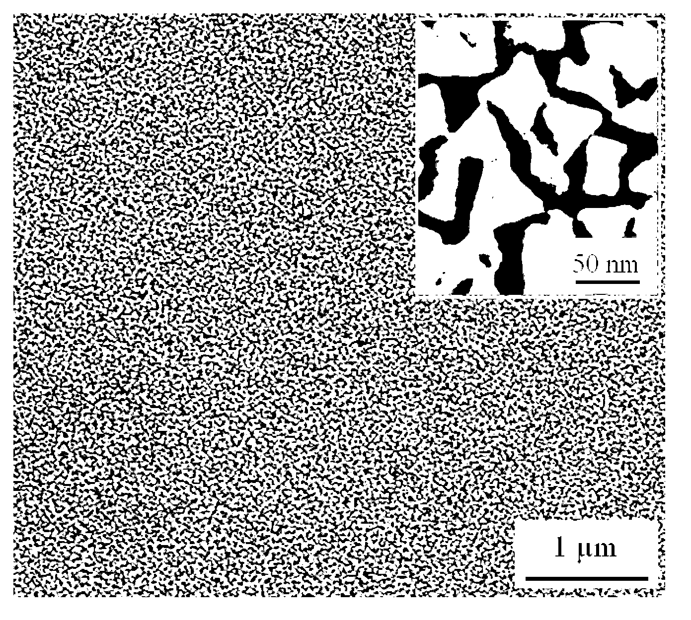
[0030] 4) Under the condition of room temperature and applied bias voltage of DC-100V, the power of RF 100W was used for further sputtering deposition of 120nm to obtain a bicontinuous "triangular ligament-hole" structure NPC thin film (see Figure 4 ). Among them, the cross-sectional size of the deltoid ligament is about 21 nm, and the pore size is about 12 nm.
[0031] figure 2 (a, b) show the surface morphologies of the pre-sputtered copper film substrates in Example 1 and Example 2, respectively. from figure 2 (a) It can be seen that the surface of the copper film substrate in Example 1 is composed of some fine particles, and their surface is relatively smooth. from figure 2 (b) It can be...
PUM
 Abstract
Description
Claims
Application Information
 - R&D Engineer
- R&D Manager
- IP Professional
- Industry Leading Data Capabilities
- Powerful AI technology
- Patent DNA Extraction
Browse by: Latest US Patents, China's latest patents, Technical Efficacy Thesaurus, Application Domain, Technology Topic, Popular Technical Reports.
© 2024 PatSnap. All rights reserved.Legal|Privacy policy|Modern Slavery Act Transparency Statement|Sitemap|About US| Contact US: help@patsnap.com