Nickel silicide layer forming method and semiconductor device forming method

A nickel silicide and semiconductor technology, which is applied in semiconductor/solid-state device manufacturing, coating, electrical components, etc., can solve the problem that the resistance of the nickel silicide layer cannot be effectively reduced, and achieve the effect of reducing resistance

Active Publication Date: 2013-04-03
SEMICON MFG INT (SHANGHAI) CORP
View PDF4 Cites 11 Cited by
  • Summary
  • Abstract
  • Description
  • Claims
  • Application Information

AI Technical Summary

Problems solved by technology

[0005] But the method of prior art still can't ef...

Method used


Image

  • Nickel silicide layer forming method and semiconductor device forming method
  • Nickel silicide layer forming method and semiconductor device forming method
  • Nickel silicide layer forming method and semiconductor device forming method

Examples


Embodiment Construction

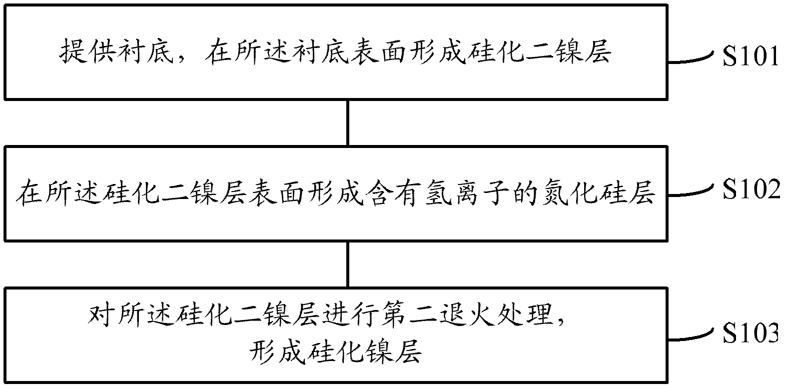
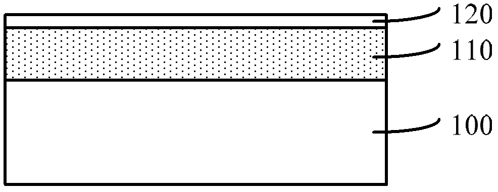
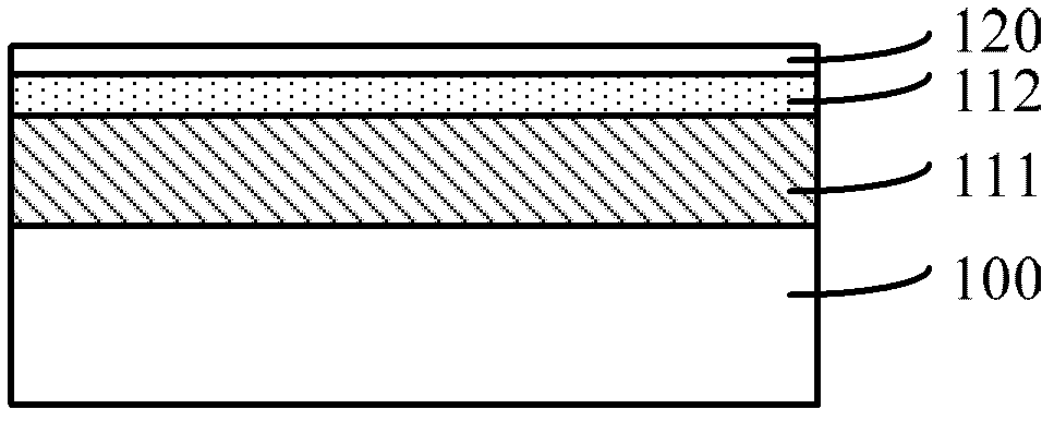
[0051]Since the prior art cannot effectively reduce the resistance of the nickel silicide layer, the RC delay of the circuit becomes larger. After research, the inventor proposes a method for forming a nickel silicide layer that can effectively reduce the resistance of the nickel silicide layer, including: providing A substrate, forming a dinickel silicide layer on the surface of the substrate; forming a silicon nitride layer containing hydrogen ions on the surface of the dinickel silicide layer; performing a second annealing treatment on the dinickel silicide layer to form a nickel silicide layer . Since the hydrogen ions in the silicon nitride layer will diffuse into the nickel silicide layer during the second annealing treatment, the sheet resistance of the nickel silicide layer containing hydrogen ions is thinner than that of the nickel silicide layer not containing hydrogen ions. The layer resistance is small, and the contact resistance between the nickel silicide layer a...


PUM


Abstract

The invention discloses a nickel silicide layer forming method and a semiconductor device forming method, wherein the nickel silicide layer forming method comprises the following steps of: providing a substrate, and forming a dinickel silicide layer on the surface of the substrate; forming a hydrogen ion containing silicon nitride layer on the surface of the dinickel silicide layer; and carrying out secondary annealing treatment on the dinickel silicide layer so as to form a nickel silicide layer. Before the step of carrying out secondary annealing treatment on the dinickel silicide layer so as to form a nickel silicide layer, a hydrogen ion containing silicon nitride layer is formed on the surface of the dinickel silicide layer, and in the process of carrying out secondary annealing treatment, hydrogen ions in the silicon nitride layer are diffused into the dinickel silicide layer, so that the finally formed nickel silicide layer internally contains hydrogen ions, therefore, the resistance of the nickel silicide layer can be effectively decreased, and the RC delay of a circuit can be reduced.

Description

technical field [0001] The invention relates to the field of semiconductor manufacturing, in particular to a method for forming a nickel silicide layer and a method for forming a semiconductor device. Background technique [0002] As the integration level of semiconductor devices continues to increase, the critical dimensions related to semiconductor devices continue to decrease, the impact of device parasitic resistance and parasitic capacitance on device performance becomes more and more significant, and the RC (resistance, capacitance) delay becomes more and more serious. Therefore, the low-resistivity interconnect structure becomes a key element in the manufacture of highly integrated semiconductor devices. Metal silicide and self-aligned metal silicide and their formation processes have been widely used to reduce the resistance of the gate, source, and drain of MOS transistors, including sheet resistance and contact resistance, thereby reducing RC delay time. In the ex...

Claims


Application Information

Patent Timeline
IPC IPC(8): C23C16/42C23C16/34C23C16/44C23C16/56H01L21/285H01L21/768
Inventor 鲍宇
Owner SEMICON MFG INT (SHANGHAI) CORP
Why Eureka
Try Eureka