

Wafer level chip size package and manufacturing method thereof
A wafer-level chip and size packaging technology, which is applied in semiconductor/solid-state device manufacturing, radiation control devices, electrical components, etc. Problems such as layer phenomenon, to improve product reliability, production efficiency, improve warpage, and reduce costs
- Summary
- Abstract
- Description
- Claims
- Application Information
AI Technical Summary
Problems solved by technology
Method used
Image

Examples
Embodiment Construction
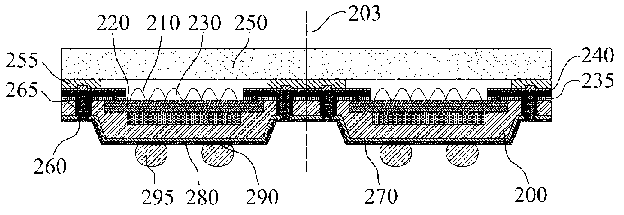
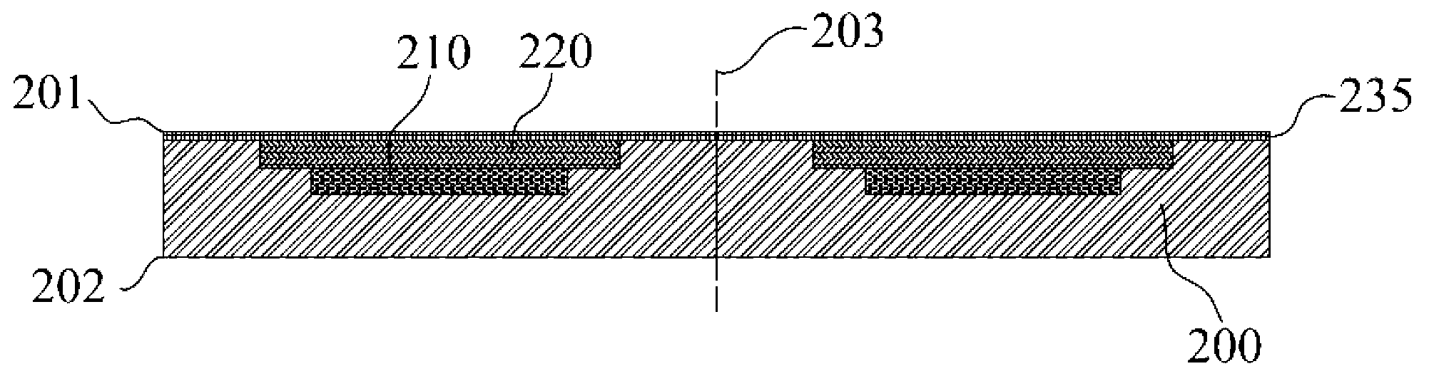
[0038] The present invention enhances the bonding force between the glass 250 and the wafer 200 by making a stepped protrusion or groove structure on the first surface 201 of the wafer, improves the delamination problem between the glass and the wafer, and improves the reliability of the package. characteristics and fit into larger size CIS packages. At the same time, the trench structure is formed by etching the second surface 202 of the wafer, which reduces the requirement for high aspect ratio through-silicon vias (TSVs). figure 2 It is a schematic diagram of a CIS package of a stepped protrusion structure fabricated on the first surface 201 of the wafer according to an embodiment of the present invention.
[0039] by figure 2 As shown, the wafer level chip scale package (WLCSP) according to the embodiment of the present invention includes a wafer 200, the front side of the wafer 200 is the first surface 201 forming the image sensing area, and the negative side of the wa...
PUM
 Abstract
Description
Claims
Application Information